RZ Family / RZ/G, RZ/A Series 2. Functional Specifications
R01UH0990EJ0101 Rev.1.01 Page 50 of 83
Jul 28, 2022
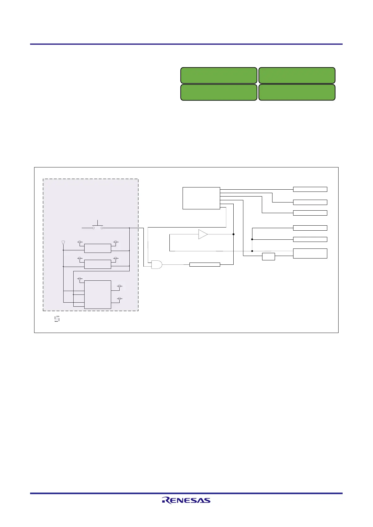
2.7 Reset Control
Figure 2.8 shows block diagrams of a reset control for the RTK9743U11S01000BE (Evaluation board Kit for
RZ/G2UL MPU).
For the RTK9743U11C01000BE, the interfaces of DDR4 SDRAM, QSPI flash memory, eMMC memory, Ethernet and
Debug are controlled by reset signal from the PMIC.
There are two types of system resets: power-on reset and reset by the button switch.
RST_#
eMMC memory
nRESET
JTAG conn
RESET_N
Ethernet PHY_0
Ethernet PHY_1
RESET#
QSPI flash memory
RESET_N
DDR4 SDRAM
RESET_IN#
RESET_BTN#
VIN VOUT
ENABLE PG
VIN VOUT
ENABLE PG
VIN
EN1 OUT1
FLT1
EN2 OUT2
FLT2
5.0V
3.3V
5.0V
CARRIER_PWR_ON
1.8V
5V_BOARD
5V_PMOD
3.3V
RZ/G2UL
ISL80102
ISL80102
ISL61852
Note: shows the Carrier Board
RESET_N
1.8V->3.3V
NRESET
DDR_RESET#
SD0_RESET#
QSPI_RESET#
PRST#
TRST#
PMIC
GNDDetect(TRST#)
PRESET#_18
WDTOVF_PERROUT#
DNF*
* You can use reset signal(TRST#) from JTAG.
If you want to use TRST# signal, please see the section2.9
SLG7RN45356

 Loading...


