5-1
SECTION 5
PRINTED WIRING BOARD
5-1. THIS NOTE IS COMMON FOR PRINTED WIRING BOARDS
2 1
3
2 1
3
2 1
3
3 4 5
2 1
1 2 3
5 4
E B
C
3 1
5
2
4 6
1 2 3
5 4
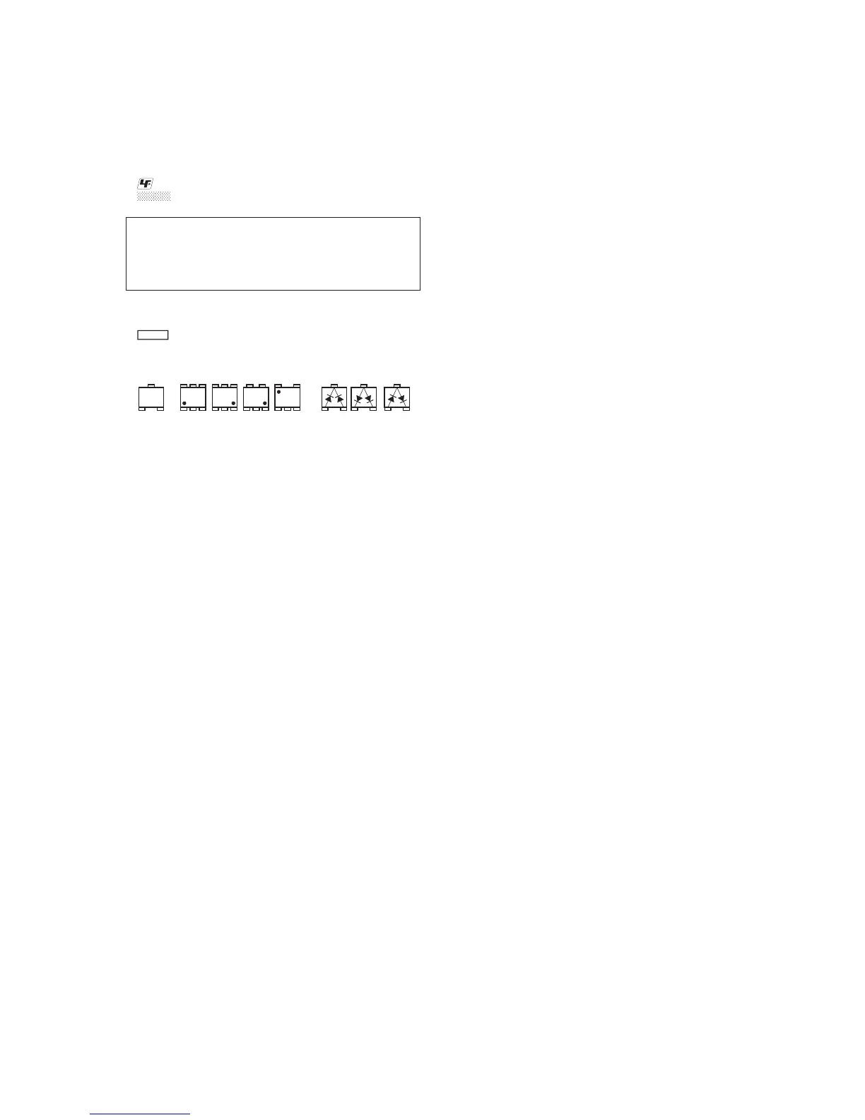
Transistor Diode
•
: Uses unleaded solders.
•
: Pattern from the side which enables seeing.
(The other layers’ patterns are not indicated)
• Through hole is omitted.
• There are few cases that the part printed on diagram isn’t mounted
in this model.
•
: panel designation
• Chip parts.
Caution:
Pattern face side:
(SIDE B)
Parts face side:
(SIDE A)
Parts on the pattern face side seen from
the pattern face are indicated.
Parts on the parts face side seen from
the parts face are indicated.
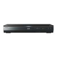
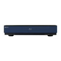
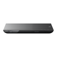
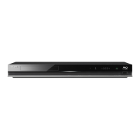
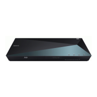
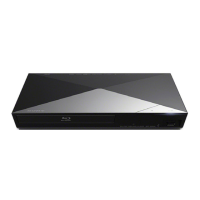
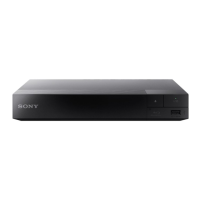
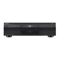
BDP-BX58/S480/S483/S580
 Loading...