4-67
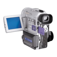
DCR-PC109/PC109E
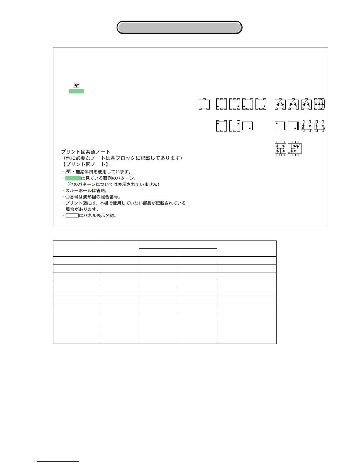
4-3. PRINTED WIRING BOARDS
4-3. PRINTED WIRING BOARDS
(For printed wiring boards)
•
: Uses unleaded solder.
•
: Pattern from the side which enables seeing.
(The other layers’ patterns are not indicated)
• Through hole is omitted.
• Circled numbers refer to waveforms.
• There are a few cases that the part printed on diagram
isn’t mounted in this model.
• C: panel designation
(ENGLISH)
THIS NOTE IS COMMON FOR WIRING BOARDS
(In addition to this, the necessary note is printed in each block)
21
3
21
3
21
3
345
21
123
654
EB
C
31
5
5
2
46
123
54
43
12
5
4
1
3
12
43
312
45
534
12
34
21
12
43
46
2
5
31
12
4
3
64
1
3
• Chip parts
Transistor Diode
(JAPANESE)
board name
CD-494
IR-052
CR-047
LB-096
SE-140
PD-213
MS-201
VC-352
parts location
(shown on page)
4-85
–
4-85
–
4-85
4-86
4-86
4-87,88
number of layers
2
2
2
2
2
2
2
8
layers not shown
–
–
–
–
–
–
–
2 to 7
CSP IC
–
–
–
–
–
–
–
IC2301, IC5001, IC5101,
IC5201, IC6201, IC6202,
IC6301, IC6401, IC7601,
IC8201, IC8401, IC8502,
IC8503, IC8801, IC9101
pattern
BOARD INFORMATION
 Loading...