M2000-00
T2000-A70 Data Modem Kit
8.15.5
Copyright TEL 31/12/97
8.15.4 Signal Specifications
Data Interface Decoupling PCB
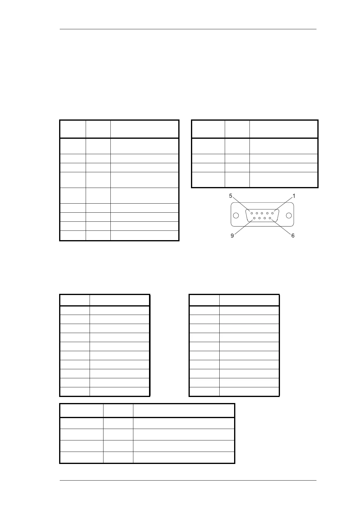
The following tables describe the signals on the decoupling PCB 9 way D-range connec-
tor (SKT1) and 4 way connector (SKT2). The diagram shows the pin designations of
SKT1, viewed from the rear of the radio.
Note:
Pins 1, 4, 6, 7, 8 and 9 on SKT1 are connected to I/O pads, so that additional sig-
nals can be interfaced to the radio through the external connector.
Figure 8.15.5 9 Way D-Range Connector (SKT1)
Data Modem PCB
The following tables describe the signals on the data modem PCB connectors P3 and
PDL-1. For P3 signal descriptions, refer to Section 5.9, “Options Interface Specifica-
tions”.
SKT1
Pin No.
Signal Description
SKT2
Pin No.
Signal Description
1 PAD1 Spare 1 DGND Ground reference for all
digital signals
2 TXD Transmit data 2 RXD Receive data
3 RXD Receive data 3 TXD Transmit data
4 PAD2 Spare 4 DGND Ground reference for all
digital signals
5 DGND Ground reference for all
digital signals
.
6PAD3Spare
7RTSSpare
8CTSSpare
9PAD4Spare
P3 Pin No. Signal P3 Pin No. Signal
1BCD-0 11/PTT-TO-OPT
2BCD-1 12/RX-GATE
3BCD-2 13/IN-LOCK
4 BCD-3 14 /PTT-FRM-OPT
5BCD-4 15/SIG-SQUELCH
6 BCD-5 16 MIC-MUTE
7TX-SIG-IN 17 DGND
8DET-AF-OUT 18 PWR-CTRL
9/BUSY 19GND
10 N/C 20 +5V
PDL-1 Pin No. Signal Description
1 DGND Ground reference for all digital signals
2 TXD Transmit data
3RXDReceive data
4 DGND Ground reference for all digital signals
 Loading...