Section
3-213
Service
THEORY
OF
OPERATION
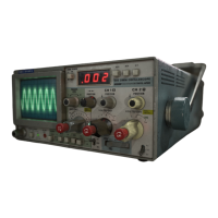
This section
of
the
manual contains a description
of
the
circuitry used
in
the
213
DMM-Oscilloscope. The description begins
with a discussion
of
the
instrument
using
the
Block Diagram pullout page
in
the
Diagrams section. Then, each circuit
is
des-
cribed
in
detail using additional detailed diagrams and the schematics
in
the
Diagrams section.
The
detailed diagrams contain
the
same
component
designations
as
the
schematics; therefore, refer
to
the
schematics for
component
electrical values and
relationships.
The
schematic being described
is
identified by its Diagrams section number (e.g.
<€))
following the first para-
graph title
that
begins
the
description of a particular schematic.
DIGITAL
LOG.IC
Digital logic techniques are used
to
perform some functions
within this instrument. The function and operation
of
the
logic circuits are described using logic symbology and termi-
nology. All logic functions are described using
the
positive
logic convention. Positive logic
is
a system
of
notation
where
the
more positive
of
two
levels
is
called
the
true, HI,
or
1 state and
the
more negative level
is
called
the
false, LO,
or O state.
The
HI-LO
method
of
notation
is
used
in
the
lo-
gic descriptions
in
this manual.
The
specific voltages which
constitute
the
HI
or
LO
state may vary between individual
devices.
It should be
noted
that
not
all
of
the
integrated circuit
de
-
vices
in
this
instrument
are digital logic devices.
The
func-
tion
of
non-digital devices are described individually using
detailed diagrams or
other
techniques
to
illustrate their
functions.
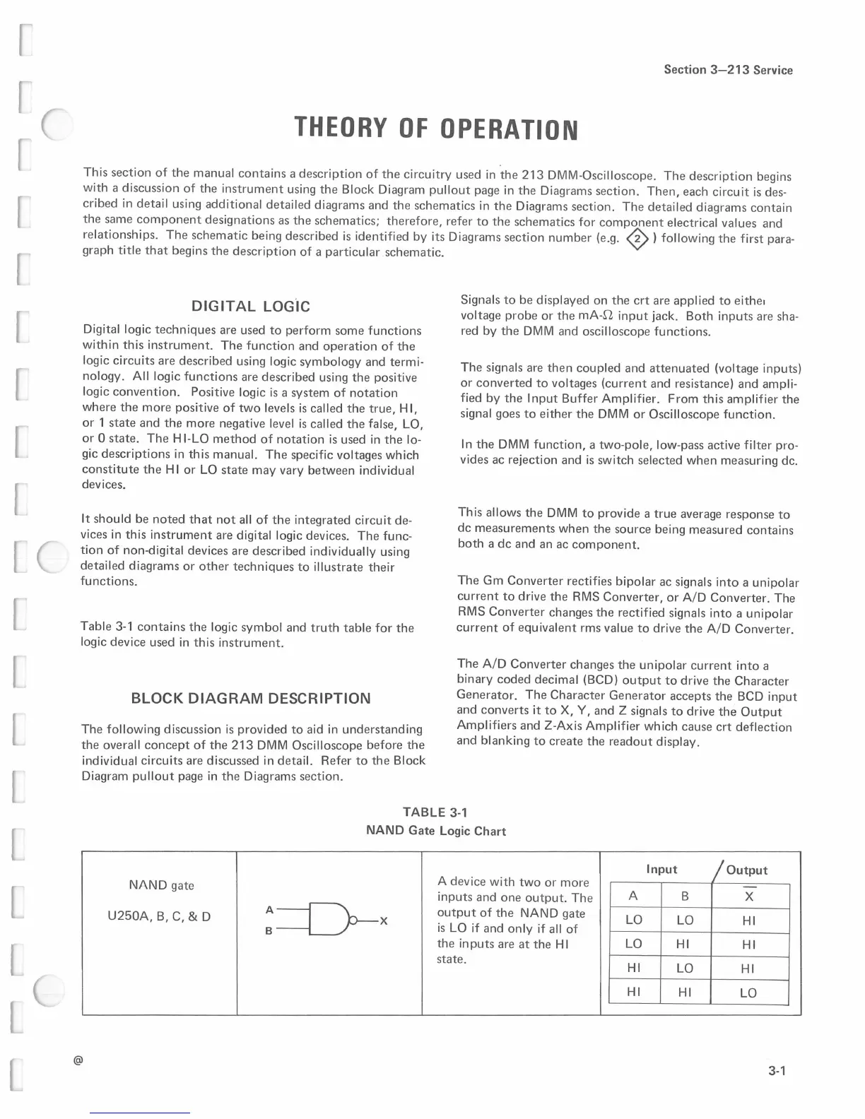
Table
3-1
contains
the
logic symbol and
truth
table for
the
logic device used
in
this instrument.
BLOCK
DIAGRAM
DESCRIPTION
The following discussion
is
provided
to
aid
in
understanding
the overall
concept
of
the
213 DMM Oscilloscope before
the
individual circuits are discussed
in
detail. Refer
to
the
Block
Diagram
pullout
page
in
the
Diagrams section.
Signals
to
be displayed on
the
crt
are applied
to
either
voltage probe or
the
mA-n
input
jack. Both inputs are sha-
red by
the
DMM
and oscilloscope functions.
The signals are
then
coupled and
attenuated
(voltage inputs)
or converted
to
voltages (current and resistance) and ampli-
fied by
the
Input Buffer Amplifier. From this amplifier the
signal goes
to
either the
DMM
or
Oscilloscope function.
In
the
DMM
function, a two-pole, low-pass active filter pro-
vides ac rejection and
is
switch selected when measuring de.
This allows the
DMM
to
provide a
true
average response
to
de measurements when the source being measured contains
both
a
de
and an ac
component.
The Gm Converter rectifies bipolar ac signals into a unipolar
current
to
drive
the
RMS
Converter,
or
A/D Converter. The
RMS
Converter changes
the
rectified signals into a unipolar
current
of
equivalent rms value
to
drive the A/D Converter.
The A/D Converter changes the unipolar
current
into a
binary coded decimal (BCD)
output
to
drive the Character
Generator. The Character Generator accepts the
BCD
input
and converts it
to
X, Y, and Z signals
to
drive
the
Output
Amplifiers and Z-Axis Amplifier which cause
crt
deflection
and blanking
to
create
the
readout
display.
TABLE
3-1
NAND
Gate
Logic
Chart
Input
/
Output
N/\ND gate
A device with
two
or more
inputs and
one
output.
The
A
B
X
U250A,
B,
C,
& D
;==[}-x
output
of
the
NANO gate
LO
LO
HI
is
LO
if
and only
if
all
of
the
in
puts are
at
the
HI
LO
HI
HI
state.
HI
LO
HI
HI
HI
LO
@
3-1
 Loading...