213
Service
iv
LIST
OF
ILLUSTRATIONS
FIGURE NO.
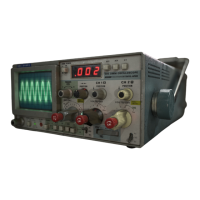
Frontispiece
213
DMM
Oscilloscope.
1-1
Dimensional Drawing
2-1
Side panel.
2-2
Front
panel.
2-3 Rear panel.
2-4 Probe storage.
2-5 Probe Body Assembly identification.
3-1
Ohms Converter detailed block diagram.
3-2 RMS Converter detailed block diagram.
3-3
A/D Converter detailed block diagram.
3-4 A/D Converter timing diagram.
3-5 Character
Generator
Z-axis
output.
3-6 Overrange circuitry simplified schematic diagram.
3-7 Overrange timing diagram.
3-8 Power
Supply
detailed block diagram.
4-1
Typical cam switch.
4-2 Circuit board locator.
4-3 Location
of
screw securing cabinet halves.
4-4
Power cord and
probe
lead routing.
4-5 Power
Supply
Board disassembly.
4-6
Attenuator
and
Function
Board disassembly.
4-7 Secondary Power Supply disassembly.
4-8 Power-I ine fuse location.
4-9
Current (mA)
input
fuse location.
4-10 Terminal
connector
holder.
4-11
Installation
of
extender
cards.
4-12 EIA color
code
example.
Section 9 figures are located near their associated diagrams
on
the
foldout
pages.
9-1
9-2
9-3
9-4
9-5
9-6
9-7
9-8
Semiconductor
lead configurations.
Power
Supply
test
points and
adjustment
locations.
Side Panel
adjustment
locations.
A/D Converter circuit board
adjustment
locations.
Block Diagram.
A 1
Attenuator
circuit board (grid locator).
A2
Function
circuit board (grid locator).
A 1
Attenuator
circuit board voltage and waveform
test
points.
PAGE
vi
1-10
2-1
2-2
2-3
2-3
2-4
3-3
3-4
3-5
3-6
3-7
3-8
3-9
3-12
4-2
4-3
4-4
4-4
4-7
4-8
4-9
4-11
4-11
4-12
4-14
4-16
@
 Loading...