www.ti.com
J721E EVM Hardware Architecture
55
SPRUIS4A–December 2019–Revised May 2020
Submit Documentation Feedback
Copyright © 2019–2020, Texas Instruments Incorporated
Jacinto7 J721E/DRA829/TDA4VM Evaluation Module (EVM)
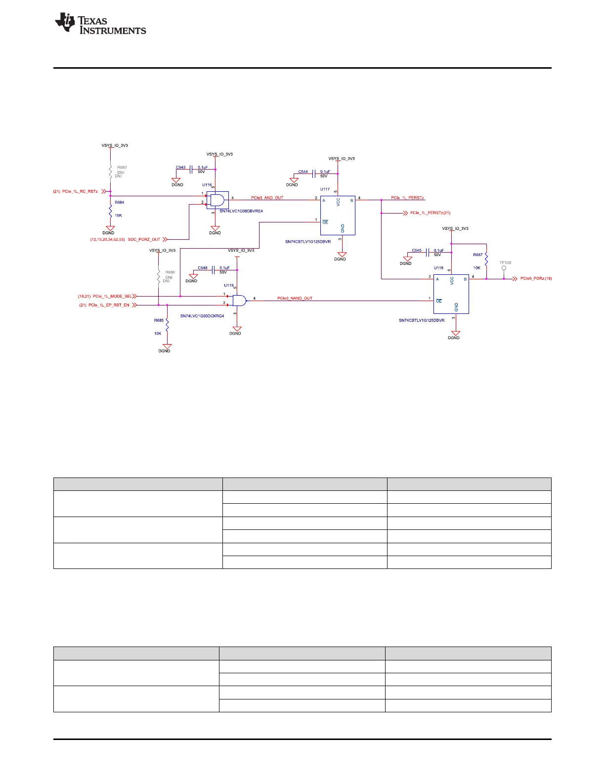
Reset: A dip Switch is provided to select the reset source for host and end-point PCIe operation. In case
of host mode, signal from GPIO Expander and PORz signals from SoC are ANDed and the output is
connected to PCIe connector. The GPIO signal is pulled low to ensure PCIe Reset (#PERST) remains
asserted until SoC releases reset.
Whereas, in case of PCIe end point operation, the CP board receives reset signal from the PCIe card.
Figure 36. 1L-PCIe Root Complex/Endpoint Selection Circuit
Clock: A clock generator (CDCI #1) is provided to drive 100 MHz HCSL clock for PCIe add on cards and
SoC. Resistor options are provided to select the clock source for host and end point operation.
For PCIe host operation:
• The add on cards can have clocks driven by SOC or clock generator. Selection can be made through
resistors as shown in Table 28.
Table 28. Reference Clock Selection for PCIe Host Operation
Clock Selected Mount Unmount
Reference Clock for SOC from clock
generator
R194 R195, C92
R198 R199, C93
Reference Clock for PCIe connector from
SOC
R195, C92 R194, R109
R199, C93 R198, R110
Reference Clock for PCIe connector from
clock generator
R109 R195, C92
R110 R199, C93
For PCIe Endpoint operation:
• The SOC can have the clock driven by add on cards or clock generator. Selection can be made
through resistors as shown in Table 29.
Table 29. Reference Clock Selection for PCIe Endpoint Operation
Clock Selected Mount Unmount
Reference clock for SOC from clock
generator
R194 R195, C92
R198 R199, C93
Reference clock for SOC from PCIe
connector
R195, C92 R194, R109
R199, C93 R198, R110

 Loading...


