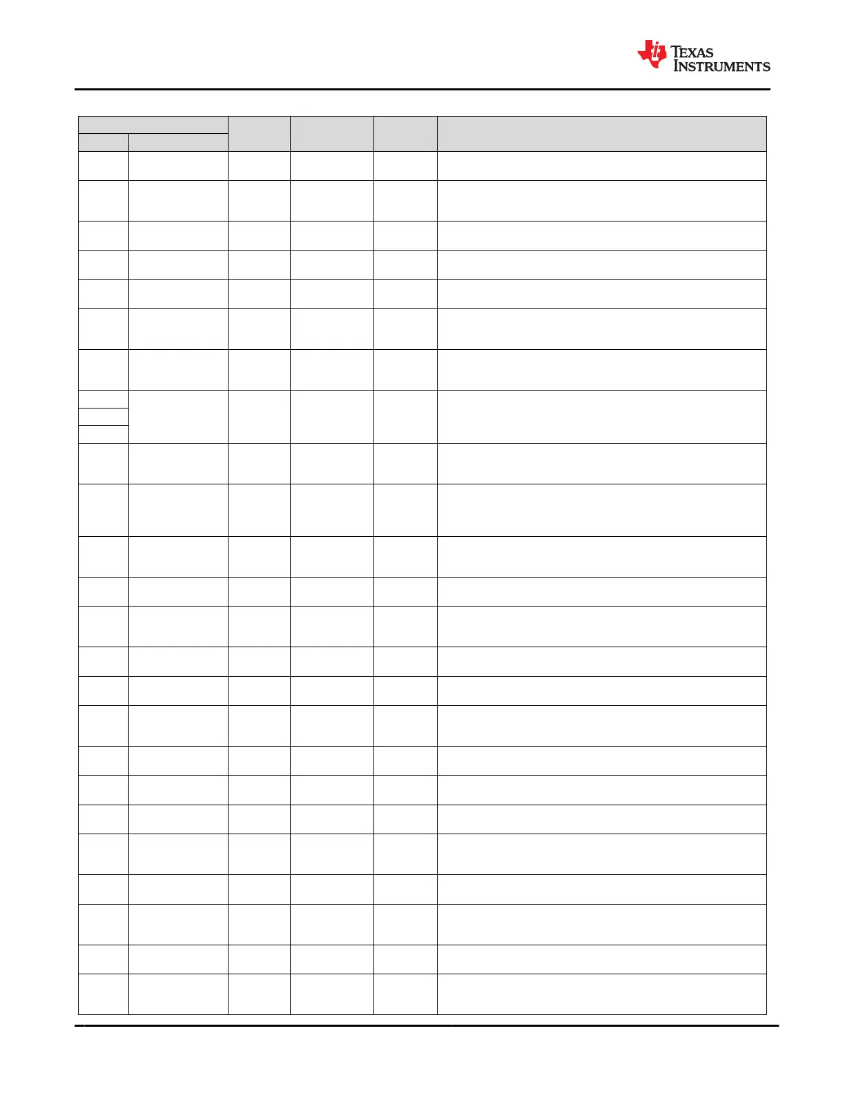
Table 6-1. Pin Functions
PIN
TYPE CATEGORY POR STATE DESCRIPTION
NO. NAME
A1 GND Ground
Ground and no
connect pins
— Ground. Connect all balls to ground plane.
A10 SENSEN Analog input
External HV-FET
control and sense
pins and soft start
Analog input
Positive sense for external high-voltage power-path current-sense
resistance. Short pin to VBUS when unused.
A11 PP_5V0 Power
High-current
power pins
—
5-V supply for VBUS. Bypass with capacitance CPP_5V0 to GND. Tie pin
to GND when unused.
A2 LDO_1V8D Power
Low-current
power pins
—
Output of the 1.8-V LDO for core digital circuits. Bypass with capacitance
CLDO_1V8D to GND.
A3 SPI_CLK
Digital
output
Digital core I/O
and control pins
Digital input SPI serial clock. Ground pin when unused
A4 SPI_POCI Digital input
Digital core I/O
and control pins
Digital input
SPI serial controller input from peripheral. This pin is used during boot
sequence to determine if the flash memory is valid. Refer to the Boot Code
section for more details. Ground pin when unused.
A5 I2C_SDA2 Digital I/O
Digital core I/O
and control pins
Digital input
I
2
C port 2 serial data. Open-drain output. Tie pin to LDO_3V3 or VDDIO
(depending on configuration) through a 10-kΩ resistance when used or
unused.
A6
PP_HV Power
High-current
power pins
—
HV supply for VBUS. Bypass with capacitance CPP_HV to GND. Tie pin to
GND when unused.
A7
A8
A9 HV_GATE2
Analog
output
External HV-FET
control and sense
pins and soft start
Short to
VBUS
External NFET gate control for high-voltage power path. Float pin when
unused.
B1 VDDIO Power
Low-current
power pins
—
VDD for I/O. Some I/Os are reconfigurable to be powered from VDDIO
instead of LDO_3V3. When VDDIO is not used, tie pin to LDO_3V3. When
not tied to LDO_3V3 and used as a supply input, bypass with capacitance
CVDDIO to GND.
B10 SENSEP Analog input
External HV-FET
control and sense
pins and soft start
Analog input
Positive sense for external high-voltage power-path current-sense
resistance. Short pin to VBUS when unused.
B11 PP_5V0 Power
High-current
power pins
—
5-V supply for VBUS. Bypass with capacitance CPP_5V0 to GND. Tie pin
to GND when unused.
B2 GPIO0 Digital I/O
Digital core I/O
and control pins
Hi-Z
General purpose digital I/O 0. Float pin if it is configured as a push-pull
output in the application. Ground pin with a 1-MΩ resistor when unused in
the application.
B3 SPI_CSZ
Digital
output
Digital core I/O
and control pins
Digital input SPI chipselect. Ground pin when unused.
B4 SPI_PICO
Digital
output
Digital core I/O
and control pins
Digital input SPI serial controller output to peripheral. Ground pin when unused.
B5 I2C_SCL2 Digital I/O
Digital core I/O
and control pins
Digital input
I
2
C port 2 serial clock. Open-drain output. Tie pin to LDO_3V3 or VDDIO
(depending on configuration) through a 10-kΩ resistance when used or
unused.
B6 I2C_IRQ2Z
Digital
output
Digital core I/O
and control pins
Hi-Z
I
2
C port 2 interrupt. Active-low. Implement externally as an open-drain with
a pullup resistance. Float pin when unused.
B7 PP_HV Power
High-current
power pins
—
HV supply for VBUS. Bypass with capacitance CPP_HV to GND. Tie pin to
GND when unused.
B8 GND Ground
Ground and no
connect pins
— Ground. Connect all balls to ground plane.
B9 HV_GATE1
Analog
output
External HV-FET
control and sense
pins and soft start
Short to
SENSEP
External NFET gate control for high-voltage power path. Float pin when
unused.
C1 I2C_IRQ1Z
Digital
output
Digital core I/O
and control pins
Hi-Z
I
2
C port 1 interrupt. Active-low. Implement externally as an open-drain with
a pullup resistance. Float pin when unused.
C10
GPIO4
(HPD TXRX)
Digital I/O
Digital core I/O
and control pins
Hi-Z
General purpose digital I/O 4. Configured as hot-plug detect (HPD) TX,
HPD RX, or both when DisplayPort mode is supported. Ground pin with a
1-MΩ resistor when unused in the application.
C11 PP_5V0 Power
High-current
power pins
—
5-V supply for VBUS. Bypass with capacitance CPP_5V0 to GND. Tie pin
to GND when unused.
C2 GPIO1 Digital I/O
Digital core I/O
and control pins
Hi-Z
General purpose digital I/O 1. Float pin if it is configured as a push-pull
output in the application. Ground pin with a 1-MΩ resistor when unused in
the application.
TPS65982
SLVSD02E – MARCH 2015 – REVISED AUGUST 2021
www.ti.com
6 Submit Document Feedback
Copyright © 2021 Texas Instruments Incorporated
Product Folder Links: TPS65982

 Loading...