MAX-7 / NEO-7 - Hardware Integration Manual
UBX-13003704 - R09 Production Information Design
Page 18 of 52
3.2.2 Minimal design (MAX-7Q)
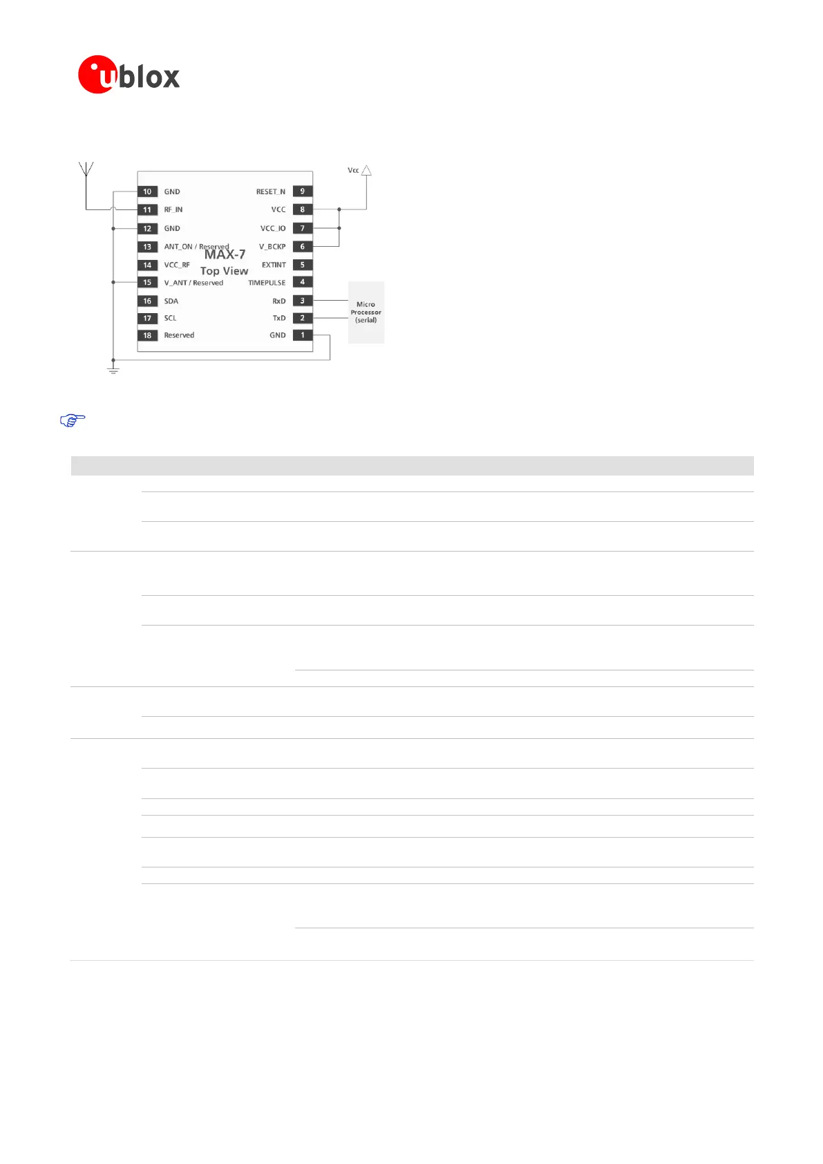
Figure 6: MAX-7 passive antenna design
For information on increasing immunity to jammers such as GSM, see section 5.3.7.
Provide clean and stable supply.
Assure a good GND connection to all GND pins of the module,
preferably with a large ground plane.
Backup supply voltage input pin. Connect to VCC_IO if not used.
GPS signal
input from
antenna
The connection to the antenna has to be routed on the PCB. Use a
controlled impedance of 50 to connect RF_IN to the antenna or
the antenna connector. DC block inside.
Output voltage
RF section
Can be used for active antenna or external LNA supply.
ANT_ON
(MAX-7C/Q)
Reserved
(MAX-7W)
ANT_ON (antenna on) HIGH can be used to turn on and LOW to
turn off an optional external LNA.
ANT_ON pin voltage level is VCC_IO
UART, leave open if not used, voltage level referred VCC_IO. Can
be configured as TX Ready indication for the DDC interface.
UART, leave open if not used, voltage level referred VCC_IO
Leave open if not used, voltage level referred VCC_IO
Leave open if not used, voltage level referred VCC_IO
DDC Data. Leave open, if not used.
DDC Clock. Leave open, if not used.
IO supply voltage. Input must be always supplied. Usually connect to
VCC pin 8
V_ANT
(MAX-7W )
Reserved
(MAX-7C/Q)
Connect to GND (or leave open) if passive antenna is used. If an
active antenna is used, add a 10 resistor in front of V_ANT input
to the Antenna Bias voltage or VCC_RF
Table 5: Pinout MAX-7

 Loading...


