LEA-6 / NEO-6 / MAX-6 - Hardware Integration Manual
UBX-14054794 Production Information Design-in
Page 41 of 85
Module
micro strip line
Ground plane
Module
micro strip line
Ground plane
PCB
PCB
Either don't use these layers or fill with ground planes
H
H
Figure 37: PCB build-up for micro strip line. Left: 2-layer PCB, right: 4-layer PCB
General design recommendations:
The length of the micro strip line should be kept as short as possible. Lengths over 2.5 cm (1 inch) should be
avoided on standard PCB material and without additional shielding.
For multi layer boards the distance between micro strip line and ground area on the top layer should at least
be as large as the dielectric thickness.
Routing the RF connection close to digital sections of the design should be avoided.
To reduce signal reflections, sharp angles in the routing of the micro strip line should be avoided. Chamfers
or fillets are preferred for rectangular routing; 45-degree routing is preferred over Manhattan style
90-degree routing.
Antenna
Antenna
Antenna
PCB
PCB
PCB
1
2
3
4
5
6
7
8
9
10
11
12
13
14
28
27
26
25
24
23
22
21
20
19
18
17
16
15
1
2
3
4
5
6
7
8
9
10
11
12
13
14
28
27
26
25
24
23
22
21
20
19
18
17
16
15
1
2
3
4
5
6
7
8
9
10
11
12
13
14
28
27
26
25
24
23
22
21
20
19
18
17
16
15
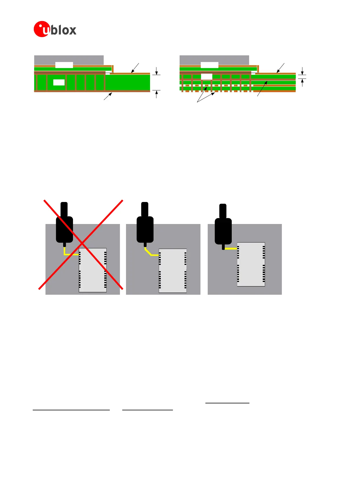
Wrong better best
Figure 38: Recommended micro strip routing to RF pin (for exact pin orientation see data sheet)
Do not route the RF-connection underneath the receiver. The distance of the micro strip line to the ground
plane on the bottom side of the receiver is very small (some 100 µm) and has huge tolerances (up to 100%).
Therefore, the impedance of this part of the trace cannot be controlled.
Use as many vias as possible to connect the ground planes.
In order to avoid reliability hazards, the area on the PCB under the receiver should be entirely covered with
solder mask. Vias should not be open. Do not route under the receiver.
2.5.4 Antenna micro strip
There are many ways to design wave-guides on printed circuit boards. Common to all is that calculation of the
electrical parameters is not straightforward. Freeware tools like AppCAD from Agilent or TXLine from Applied
Wave Research, Inc. are of great help. They can be downloaded from www.agilent.com or
http://www.hp.woodshot.com/ and www.mwoffice.com.
The micro strip is the most common configuration for printed circuit boards. The basic configuration is shown in
Figure 39 and Figure 40. As a rule of thumb, for a FR-4 material the width of the conductor is roughly double
the thickness of the dielectric to achieve 50 line impedance.

 Loading...


