SARA-R4 series - System integration manual
UBX-16029218 - R20 Design-in Page 97 of 128
C1-Public
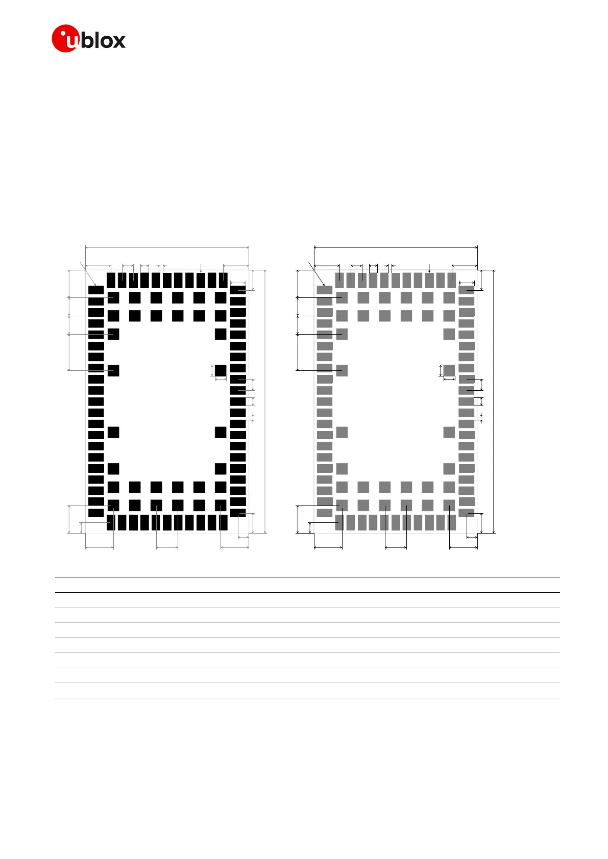
2.12 Module footprint and paste mask
Figure 67 and Table 47 describe the suggested footprint (i.e. copper mask) and paste mask layout for
SARA modules: the proposed land pattern layout reflects the modules’ pins layout, while the proposed
stencil apertures layout is slightly different (see the F’’, H’’, I’’, J’’, O’’ parameters compared to the F’,
H’, I’, J’, O’ ones).
The Non Solder resist Mask Defined (NSMD) pad type is recommended over the Solder resist Mask
Defined (SMD) pad type, as it implements the solder resist mask opening 50 µm larger per side than
the corresponding copper pad.
The recommended thickness of the stencil for the soldering paste is 150 µm, according to application
production process requirements.
Table 47: SARA-R4 series modules suggested footprint and paste mask dimensions
☞ These are recommendations only and not specifications. The exact copper, solder and paste mask
geometries, distances, stencil thicknesses and solder paste volumes must be adapted to the
specific production processes (e.g. soldering etc.) implemented.
 Loading...


