For conguraon details, see the UltraScale Architecture Conguraon User Guide (UG570). The
detailed FPGA and Flash pin connecons for the feature described in this secon are
documented in the Alveo U50 accelerator card XDC le, referenced in Appendix A: Xilinx Design
Constraints (XDC) File.
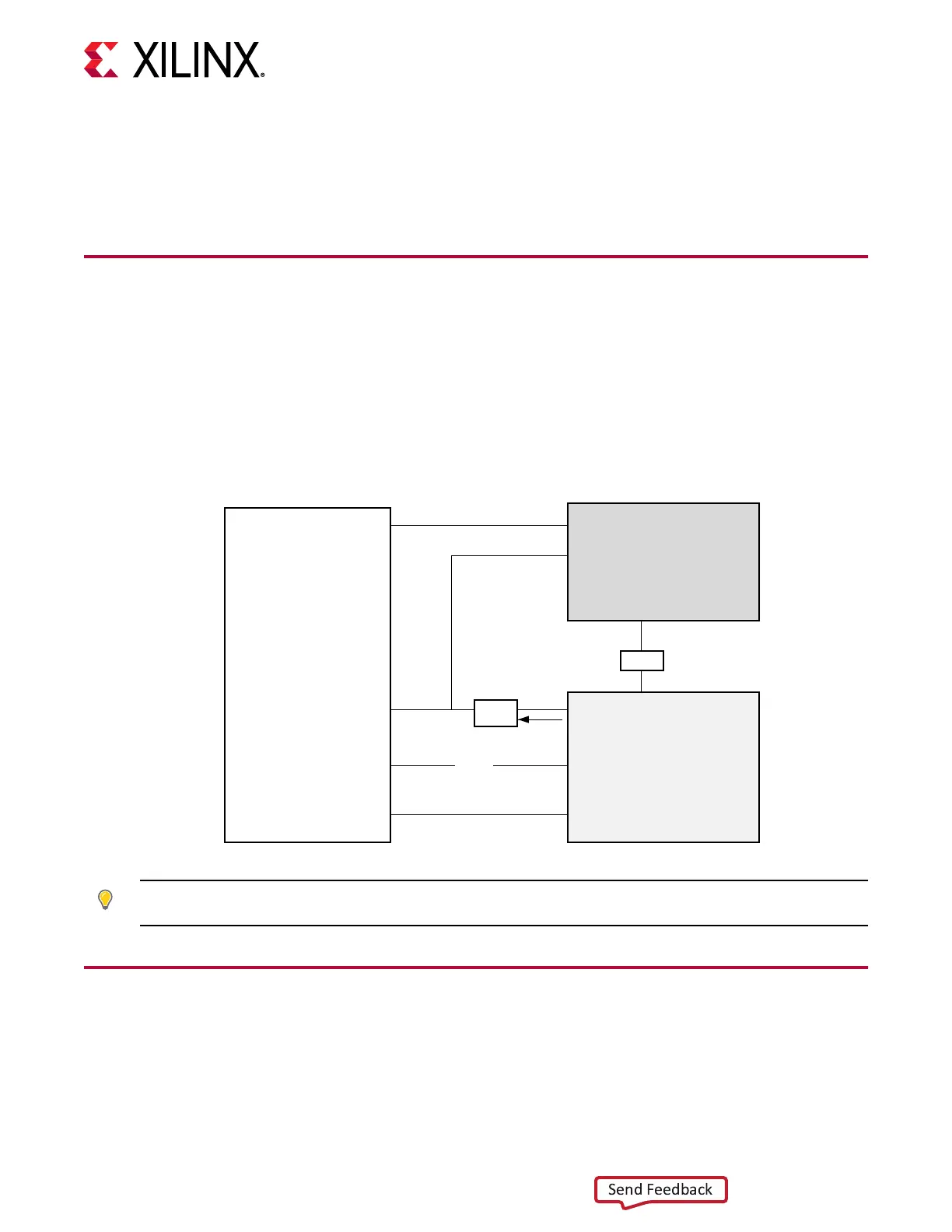
Maintenance Connector Interface
The Alveo U50 accelerator card provides access to the FPGA through the JTAG interface using a
debug and maintenance board (DMB) connected to the 30-pin maintenance connector. The
connector pinout supports three UART debug interfaces: PMBus, FPGA JTAG, and satellite
controller JTAG. The following gure shows the maintenance connector interface. For more
informaon, see Alveo Programming Cable User Guide (UG1377).
Figure 5: Maintenance Connector
Maintenance
Connector
2x15
Satellite
Controller
MSP432
JTAG1
SC_UART_RXD/TXD
FPGA_TXD/RXD_MSP
XLT
XLT
Control from SC
JTAG0
UART0
X22955-072919
XCU50
FPGA
TIP: The Alveo Programming Cable is not provided with the U50 (QSFP) producon card. This cable can be
purchased at the following link: hps://www.xilinx.com/products/boards-and-kits/alveo/accessories.html.
PCI Express Endpoint
The Alveo U50 accelerator card implements a 16-lane PCI Express edge connector that performs
data transfers at the rate of 2.5 giga-transfers per second (GT/s) for Gen1, 5.0 GT/s for Gen2, 8.0
GT/s for Gen3 applicaons, and 16.0 GT/s for Gen4 applicaons.
Chapter 4: Card Component Description
UG1371 (v1.2) December 18, 2019 www.xilinx.com
Alveo U50 Accelerator Card User Guide 17
 Loading...