Copyright © 2015 Avnet, Inc. AVNET and the AV logo are registered trademarks of Avnet, Inc. All other brands are property of their respective owners.
Avnet Electronics Marketing 3 of 28 Rev D 24 Apr 2015
Figures
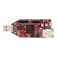
Figure 1 – Spartan-6 FPGA LX9 MicroBoard Front .............................................................................................. 6
Figure 2 – Spartan-6 FPGA LX9 MicroBoard Back .............................................................................................. 6
Figure 3 – Spartan-6 FPGA LX9 MicroBoard Block Diagram .............................................................................. 8
Figure 4 – XC6SLX9 CSG324 I/O Allocation ................................................................................................ 10
Figure 5 – Spartan-6 FPGA LX9 MicroBoard Memory Interfaces ...................................................................... 12
Figure 6 – Spartan-6 FPGA LX9 LPDDR Mobile SDRAM Interface ................................................................. 13
Figure 7 – 10/100 Ethernet Interface .................................................................................................................... 17
Figure 8 – PMOD Connector Pinout .................................................................................................................... 19
Figure 9 – TPS65708 Connections ....................................................................................................................... 21
Figure 10 – Xilinx Ribbon Cable JTAG Connector ............................................................................................. 24
Tables
Table 1 – Ordering Information .............................................................................................................................. 7
Table 2 – CDCE913 Clocks .................................................................................................................................. 11
Table 3 – CDCE913 I2C ....................................................................................................................................... 11
Table 4 – 66 MHz Clock ....................................................................................................................................... 11
Table 5 – LPDDR Timing Parameters .................................................................................................................. 14
Table 6 – FPGA SPI Interface Pinout ................................................................................................................... 15
Table 7 – USB-JTAG Signals ............................................................................................................................... 16
Table 8 – USB-to-UART Pin Locations ............................................................................................................... 16
Table 9 – 10/100 Pin Assignments ....................................................................................................................... 18
Table 10 – Peripheral Module Connections – J4 .................................................................................................. 19
Table 11 – Peripheral Module Connections – J5 .................................................................................................. 19
Table 12 – LED Pin Assignments ......................................................................................................................... 20
Table 13 – FPGA Dip Switches ............................................................................................................................ 20
Table 14 – FPGA Push Button.............................................................................................................................. 20
Table 15 – S6LX9 MicroBoard Capacitors for XC6SLX9-CSG324 ................................................................... 22
Table 16 – S6LX9 Board Capacitor Quantities for XC6SLX9-CSG324 ............................................................. 22