XC4000 Series Field Programmable Gate Arrays
4-16 September 18, 1996 (Version 1.04)
RAM Inputs and Outputs
The F1-F4 and G1-G4 inputs to the function generators act
as address lines, selecting a particular memory cell in each
look-up table.
The functionality of the CLB control signals changes when
the function generators are configured as RAM. The DIN/
H2, H1, and SR/H0 lines become the two data inputs (D0,
D1) and the Write Enable (WE) input for the 16x2 memory.
When the 32x1 configuration is selected, D1 acts as the
fifth address bit and D0 is the data input.
The contents of the memory cell(s) being addressed are
available at the F’ and G’ function-generator outputs. They
can exit the CLB through its X and Y outputs, or can be cap-
tured in the CLB flip-flop(s).
Configuring the CLB function generators as Read/Write
memory does not affect the functionality of the other por-
tions of the CLB, with the exception of the redefinition of the
control signals. In 16x2 and 16x1 modes, the H’ function
generator can be used to implement Boolean functions of
F’, G’, and D1, and the D flip-flops can latch the F’, G’, H’, or
D0 signals.
Single-Port Edge-Triggered Mode
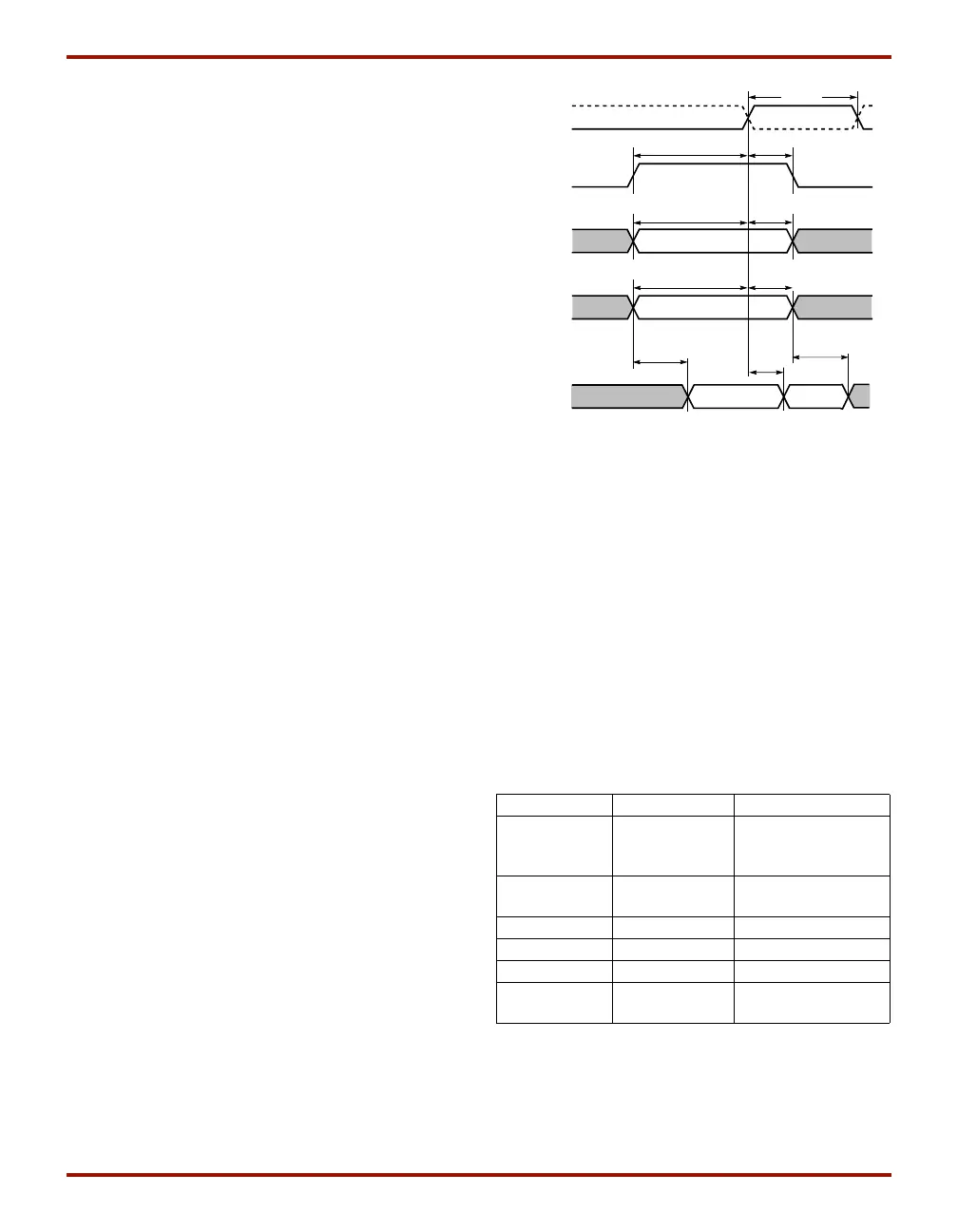
Edge-triggered (synchronous) RAM simplifies timing
requirements. XC4000-Series edge-triggered RAM timing
operates like writing to a data register. Data and address
are presented. The register is enabled for writing by a logic
High on the write enable input, WE. Then a rising or falling
clock edge loads the data into the register, as shown in
Figure 5.
Complex timing relationships between address, data, and
write enable signals are not required, and the external write
enable pulse becomes a simple clock enable. The active
edge of WCLK latches the address, input data, and WE sig-
nals. An internal write pulse is generated that performs the
write. See Figure 3 and Figure 4 for block diagrams of a
CLB configured as 16x2 and 32x1 edge-triggered, single-
port RAM.
The relationships between CLB pins and RAM inputs and
outputs for single-port, edge-triggered mode are shown in
Table 7.
The Write Clock input (WCLK) can be configured as active
on either the rising edge (default) or the falling edge. It
uses the same CLB pin (K) used to clock the CLB flip-flops,
but it can be independently inverted. Consequently, the
RAM output can optionally be registered within the same
CLB either by the same clock edge as the RAM, or by the
opposite edge of this clock. The sense of WCLK applies to
both function generators in the CLB when both are config-
ured as RAM.
The WE pin is active-High and is not invertible within the
CLB.
Note:
The pulse following the active edge of WCLK (T
WPS
in Figure 5) must be less than one millisecond wide. For
most applications, this requirement is not overly restrictive;
however, it must not be forgotten. Stopping WCLK at this
point in the write cycle could result in excessive current and
even damage to the larger devices if many CLBs are con-
figured as edge-triggered RAM.
Table 7: Single-Port Edge-Triggered RAM Signals
RAM Signal CLB Pin Function
D D0 or D1
(16x2, 16x1)
D0 (32x1)
Data In
A[3:0] F1-F4 or
G1-G4
Address
A[4] D1 (32x1) Address
WE WE Write Enable
WCLK K Clock
SPO
(Data Out)
F’ or G’ Single Port Out
(Data Out)
X6461
WCLK (K)
WE
ADDRESS
DATA IN
DATA OUT OLD NEW
T
DSS
T
DHS
T
ASS
T
AHS
T
WSS
T
WPS
T
WHS
T
WOS
T
ILO
T
ILO
Figure 5: Edge-Triggered RAM Write Timing
 Loading...