September 18, 1996 (Version 1.04) 4-177
User I/O Per Package
Maximum available user I/O for each device/package combination is shown in Table 28 - Table 30.
Pinout tables for XC4000-Series devices follow. Pinout data is offered in two forms, as device-specific and package-specific
tables. Device-specific tables include all packages for each XC4000-Series device. They follow the pad locations around
the die, and include boundary scan register locations. Package-specific tables include all XC4000-Series devices available
in a given package. These tables are especially useful in determining which pads should be avoided, in case of a future
transition to a different device in the same package.
All pinouts defined at the time of publication are included in these tables. Additional information may be available. Call your
local sales office or see the Xilinx WEBLINX at http://www.xilinx.com for the latest information.
Note: This table includes standard user-programmable I/O. It also includes the TDI, TCK, and TMS pins, which can function as
user-programmable I/O if not used for boundary scan. In addition to the I/O listed in this table, the M0 and M2 pins can be
used as inputs only; the M1 and TDO pins can be used as outputs only. All of these pins must be called out using special
library symbols. The XACT software does not use them by default. (See Table 18 on page 47.)
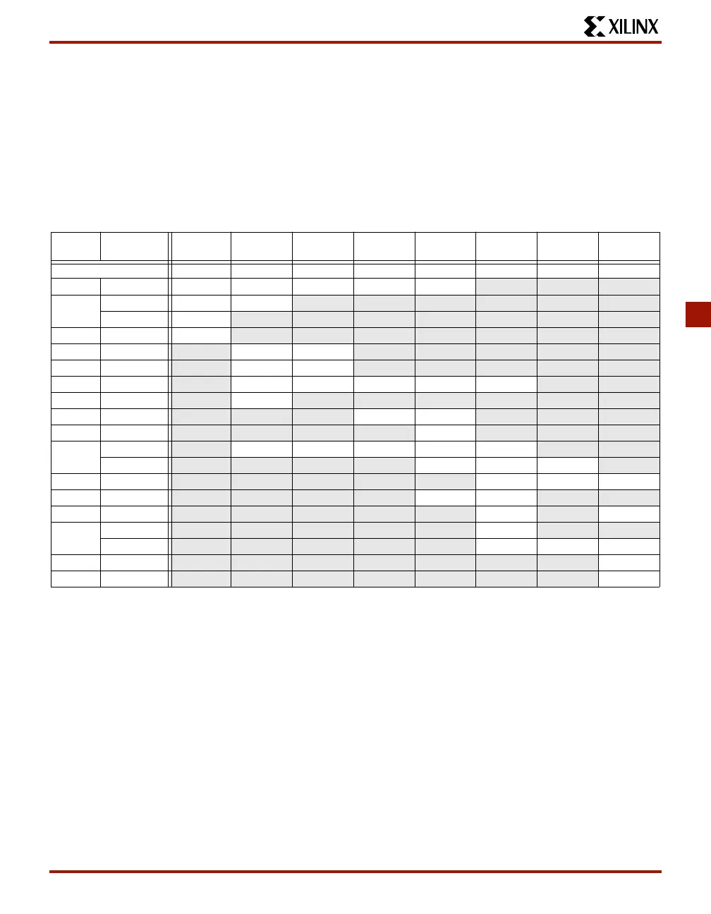
Table 28: Maximum User I/O for XC4000E Device/Package Combinations
No. of
Pins
Package
(Code)
XC4003E XC4005E XC4006E XC4008E XC4010E XC4013E XC4020E XC4025E
Maximum User I/O 80 112 128 144 160 192 224 256
84 PLCC (PC) 61 61 61 61 61
100 PQFP (PQ) 77 77
VQFP (VQ) 77
120 PGA (PG) 80
144 TQFP (TQ) 112 113
156 PGA (PG) 112 125
160 PQFP (PQ) 112 128 129 129 129
164 CBFP (CB) 112
191 PGA (PG) 144 160
196 CBFP (CB) 160
208 PQFP (PQ) 112 128 144 160 160
HQFP (HQ) 160 160 160
223 PGA (PG) 192 192 192
225 BGA (BG)
160 192
228 CBFP (CB) 192 192
240 PQFP (PQ)
192
HQFP (HQ) 192 192 193
299 PGA (PG)
256
304 HQFP (HQ)
256
 Loading...