September 18, 1996 (Version 1.04) 4-45
The Global Early buffers can be driven by either semi-ded-
icated pads or internal logic. They share pads with the Glo-
bal Low-Skew buffers, so a single net can drive both global
buffers, as described above.
To use a Global Early buffer, place a BUFGE element in a
schematic or in HDL code. If desired, attach a LOC
attribute or property to direct placement to the designated
location. For example, attach a LOC=T attribute or prop-
erty to direct that a BUFGE be placed in one of the two Glo-
bal Early buffers on the top edge of the device, or a
LOC=TR to indicate the Global Early buffer on the top edge
of the device, on the right.
FastCLK Buffers
The fastest way to bring a clock into the XC4000EX device
is through a FastCLK buffer. Two FastCLK buffers are
present on the left edge, and two on the right edge, of the
XC4000EX die. There are no FastCLK buffers on the top or
bottom edges.
One purpose of the FastCLK buffers is to create a very fast
pin-to-pin path by using the IOB 2-input function generator
in conjunction with the FastCLK. Drive the F input of the
IOB function generator with the FastCLK buffer output, as
described in “IOB Output Signals” on page 27.
Alternatively, a FastCLK buffer can be used to minimize the
setup time of device inputs, if a positive hold time is accept-
able. Use the FastCLK buffer to clock the Fast Capture
latch, and a slower clock buffer to clock the standard IOB
flip-flop or latch. Either the Global Early buffer or the Global
Low-Skew buffer can be used for the second storage ele-
ment, but whichever one is used should be the same clock
as the related internal logic. Since the FastCLK pads are
different from the Global Early and Global Low-Skew pads,
care must be taken to ensure that skew external to the
device does not create internal timing difficulties.
The FastCLK buffers can also be used to provide a fast
Clock-to-Out on device output pins. However, a fast clock
in the output flip-flop IOB must be taken into consideration
when calculating the internal clock speed for the design.
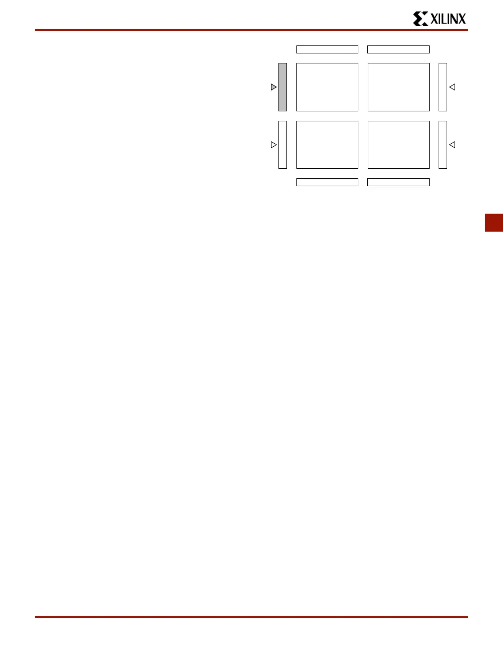
The FastCLK buffers are limited to accessing IOBs on one-
half of the die edge only, as shown in Figure 40 and
Figure 36 on page 42. They can each drive two of the four
vertical lines accessing the IOBs on the left edge of the
device, or two of the eight vertical lines accessing the IOBs
on the right edge of the device. They can only access the
CLB array through single- and double-length lines.
The FastCLK buffers must be driven by the semi-dedicated
IOBs. They are not accessible from internal nets. Other
than the FastCLK feature, these IOBs are identical to all
other IOBs.
To use a FastCLK buffer, place a BUFFCLK element in a
schematic or in HDL code. If desired, attach a LOC
attribute or property to direct placement to the designated
location. For example, attach a LOC=LB attribute or prop-
erty to direct that a BUFFCLK be placed on the left edge of
the device at the bottom, or use LOC=L to indicate either of
the buffers on the left edge.
The input to the BUFFCLK symbol must be driven by a
input pad symbol, such as IPAD, or by an input flip-flop or
latch, such as INFF, ILD, ILFFX, or ILFLX.
14
2
3
CLB CLB
CLBCLB
I
O
B
I
O
B
I
O
B
I
O
B
IOB IOB
IOBIOB
X6745
Figure 40: Each BUFFCLK Can Drive Any or
All Clock Inputs in Same Half-Edge (FCLK1 is shown.
FCLK2, FCLK3 and FCLK4 are similar.)
 Loading...