XC4000 Series Field Programmable Gate Arrays
4-46 September 18, 1996 (Version 1.04)
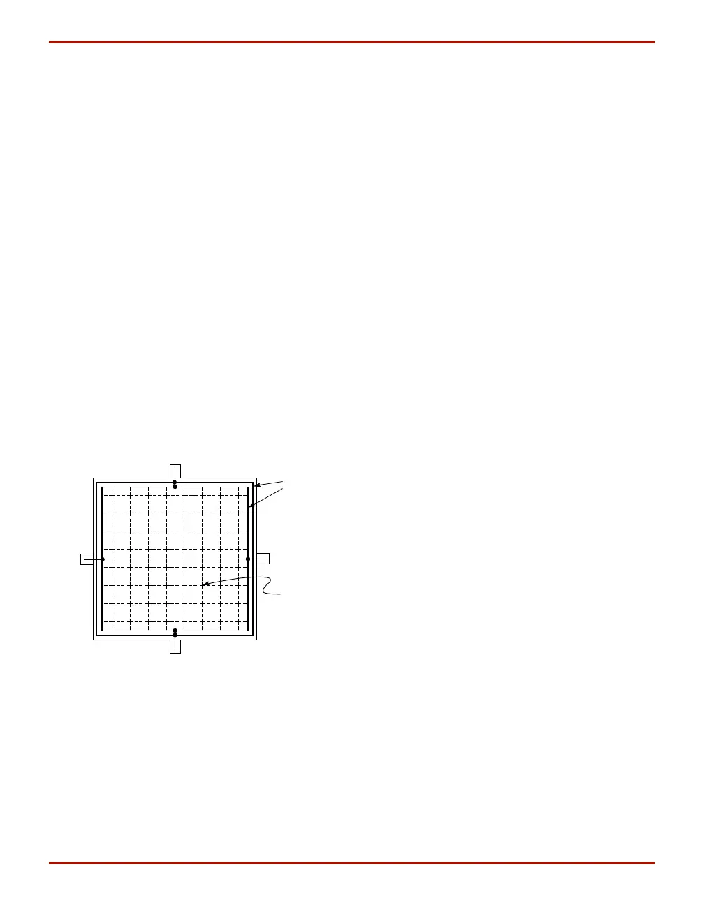
Power Distribution
Power for the FPGA is distributed through a grid to achieve
high noise immunity and isolation between logic and I/O.
Inside the FPGA, a dedicated Vcc and Ground ring sur-
rounding the logic array provides power to the I/O drivers,
as shown in Figure 41. An independent matrix of Vcc and
Ground lines supplies the interior logic of the device.
This power distribution grid provides a stable supply and
ground for all internal logic, providing the external package
power pins are all connected and appropriately decoupled.
Typically, a 0.1 µF capacitor connected near the Vcc and
Ground pins of the package will provide adequate decou-
pling.
Output buffers capable of driving/sinking the specified 12
mA (XC4000E) or 24 mA (XC4000EX) loads under speci-
fied worst-case conditions may be capable of driving/sink-
ing up to 10 times as much current under best case
conditions.
Noise can be reduced by minimizing external load capaci-
tance and reducing simultaneous output transitions in the
same direction. It may also be beneficial to locate heavily
loaded output buffers near the Ground pads. The I/O Block
output buffers have a slew-rate limited mode (default) which
should be used where output rise and fall times are not
speed-critical.
Pin Descriptions
There are three types of pins in the XC4000-Series
devices:
• Permanently dedicated pins
• User I/O pins that can have special functions
• Unrestricted user-programmable I/O pins.
Before and during configuration, all outputs not used for the
configuration process are 3-stated with a 50 kΩ - 100 kΩ
pull-up resistor.
After configuration, if an IOB is unused it is configured as
an input with a 50 kΩ - 100 kΩ pull-up resistor.
XC4000-Series devices have no dedicated Reset input.
Any user I/O can be configured to drive the Global Set/
Reset net, GSR. See “Global Set/Reset” on page 13 for
more information on GSR.
XC4000-Series devices have no Powerdown control input,
as the XC3000 and XC2000 families do. The XC3000/
XC2000 Powerdown control also 3-stated all of the device I/
O pins. For XC4000-Series devices, use the global 3-state
net, GTS, instead. This net 3-states all outputs, but does
not place the device in low-power mode. See “IOB Output
Signals” on page 27 for more information on GTS.
Device pins for XC4000-Series devices are described in
Table 18. Pin functions during configuration for each of the
seven configuration modes are summarized in Table 24 on
page 78, in the “Configuration Timing” section.
GND
Ground and
Vcc Ring for
I/O Drivers
Vcc
GND
Vcc
Logic
Power Grid
X5422
Figure 41: XC4000-Series Power Distribution
 Loading...