EasyManua.ls Logo

Xilinx XC4000 Series User Manual

Xilinx XC4000 Series
55 pages
To Next Page IconTo Next Page
To Previous Page IconTo Previous Page
Page #44 background imageLoading...
Page #44 background image
XC4000 Series Field Programmable Gate Arrays
4-48 September 18, 1996 (Version 1.04)
TDO O O
If boundary scan is used, this pin is the Test Data Output. If boundary scan is not used,
this pin is a 3-state output without a register, after configuration is completed.
This pin can be user output only when called out by special schematic definitions. To
use this pin, place the library component TDO instead of the usual pad symbol. An out-
put buffer must still be used.
TDI, TCK,
TMS
I
I/O
or I
(JTAG)
If boundary scan is used, these pins are Test Data In, Test Clock, and Test Mode Select
inputs respectively. They come directly from the pads, bypassing the IOBs. These pins
can also be used as inputs to the CLB logic after configuration is completed.
If the BSCAN symbol is not placed in the design, all boundary scan functions are inhib-
ited once configuration is completed, and these pins become user-programmable I/O.
In this case, they must be called out by special schematic definitions. To use these pins,
place the library components TDI, TCK, and TMS instead of the usual pad symbols. In-
put or output buffers must still be used.
HDC O I/O
High During Configuration (HDC) is driven High until the I/O go active. It is available as
a control output indicating that configuration is not yet completed. After configuration,
HDC is a user-programmable I/O pin.
LDC
O I/O
Low During Configuration (LDC) is driven Low until the I/O go active. It is available as a
control output indicating that configuration is not yet completed. After configuration,
LDC is a user-programmable I/O pin.
INIT
I/O I/O
Before and during configuration, INIT is a bidirectional signal. A 1 k - 10 k external
pull-up resistor is recommended.
As an active-Low open-drain output, INIT is held Low during the power stabilization and
internal clearing of the configuration memory. As an active-Low input, it can be used
to hold the FPGA in the internal WAIT state before the start of configuration. Master
mode devices stay in a WAIT state an additional 30 to 300 µs after INIT has gone High.
During configuration, a Low on this output indicates that a configuration data error has
occurred. After the I/O go active, INIT is a user-programmable I/O pin.
PGCK1 -
PGCK4
(XC4000E
only)
Weak
Pull-up
I or I/O
Four Primary Global inputs each drive a dedicated internal global net with short delay
and minimal skew. If not used to drive a global buffer, any of these pins is a user-pro-
grammable I/O.
The PGCK1-PGCK4 pins drive the four Primary Global Buffers. Any input pad symbol
connected directly to the input of a BUFGP symbol is automatically placed on one of
these pins.
SGCK1 -
SGCK4
(XC4000E
only)
Weak
Pull-up
I or I/O
Four Secondary Global inputs each drive a dedicated internal global net with short delay
and minimal skew. These internal global nets can also be driven from internal logic. If
not used to drive a global net, any of these pins is a user-programmable I/O pin.
The SGCK1-SGCK4 pins provide the shortest path to the four Secondary Global Buff-
ers. Any input pad symbol connected directly to the input of a BUFGS symbol is auto-
matically placed on one of these pins.
GCK1 -
GCK8
(XC4000EX
only)
Weak
Pull-up
I or I/O
Eight inputs can each drive a Global Low-Skew buffer. In addition, each can drive a Glo-
bal Early buffer. Each pair of global buffers can also be driven from internal logic, but
must share an input signal. If not used to drive a global buffer, any of these pins is a
user-programmable I/O.
Any input pad symbol connected directly to the input of a BUFGLS or BUFGE symbol
is automatically placed on one of these pins.
FCLK1 -
FCLK4
(XC4000EX
only)
Weak
Pull-up
I or I/O
Four FCLK inputs can each drive a FastCLK buffer. The FastCLK buffers cannot be
driven from internal logic. If not used to drive a global buffer, any of these pins is a user-
programmable I/O.
Any input pad symbol connected directly to the input of a BUFFCLK symbol is automat-
ically placed on one of these pins.
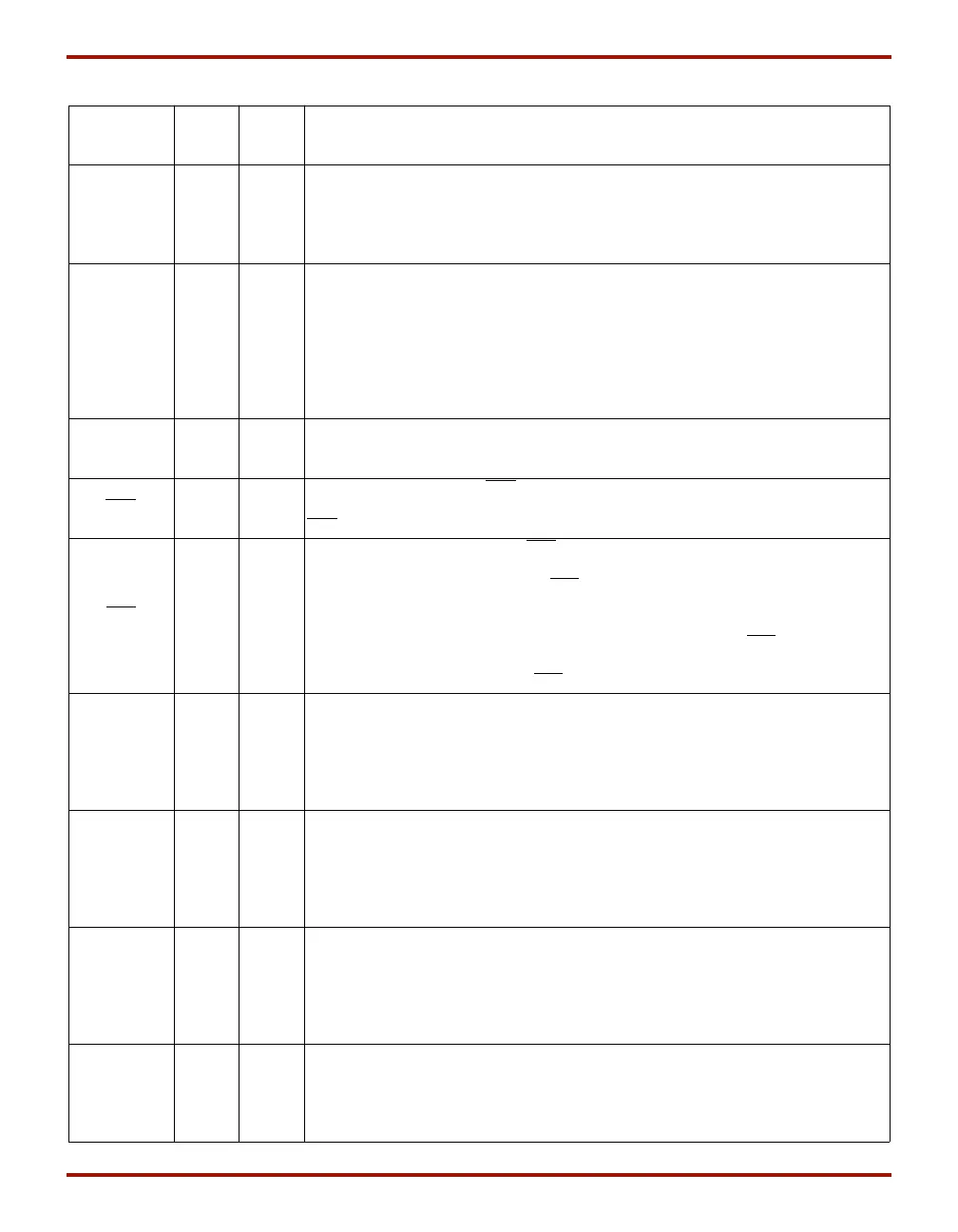
Table 18: Pin Descriptions (Continued)
Pin Name
I/O
During
Config.
I/O
After
Config. Pin Description

Table of Contents

Question and Answer IconNeed help?

Do you have a question about the Xilinx XC4000 Series and is the answer not in the manual?

Xilinx XC4000 Series Specifications

General IconGeneral
FamilyXC4000
CategoryFPGA
TechnologyCMOS
Supply Voltage5V
Operating Voltage5V
Package OptionsPGA, PQFP
Package TypesPGA, PQFP

Summary

XC4000-Series Features

Additional XC4000EX/XL Features

Details specific enhancements for XC4000EX/XL families, including higher capacity and routing.

Low-Voltage Versions Available

Information on low-voltage XC4000L and XC4000XL device variants.

Introduction

Overview of XC4000-Series FPGAs, their benefits, and history.

Description

General description of the XC4000-Series architecture, software support, and applications.

Taking Advantage of Reconfiguration

XC4000E and XC4000EX Families Compared to the XC4000

Increased System Speed

Discusses performance improvements in XC4000E/EX over older families, citing MHz rates.

PCI Compliance

States that XC4000-Series -3 and faster speed grades are PCI compliant.

Carry Logic

Details the significantly faster carry logic chain in XC4000-Series devices.

Select-RAM Memory: Edge-Triggered, Synchronous RAM Modes

Describes the on-chip RAM configuration options for synchronous and edge-triggered writes.

Dual-Port RAM

Explains the dual-port RAM option for 16x1 configurations within CLBs.

IOB Clock Enable

Covers the common clock enable input for IOB flip-flops, enhancing versatility.

Input Thresholds

Discusses globally configurable input thresholds for TTL and CMOS levels.

Global Signal Access to Logic

Configuration Pin Pull-Up Resistors

Soft Start-up

XC4000 and XC4000A Compatibility

Additional Improvements in XC4000EX Only

Increased Routing

Highlights additional vertical and horizontal interconnect lines in the XC4000EX.

Faster Input and Output

Covers dedicated early clock buffers for fast input data capture and output.

Latch Capability in CLBs

Notes the ability to configure CLB storage elements as latches in XC4000EX.

IOB Output MUX From Output Clock

Describes the IOB output multiplexer for pad sharing or 2-input function generation.

Express Configuration Mode

Introduces a new slave configuration mode accepting parallel data input for faster rates.

Additional Address Bits

Mentions extended addressing in Master Parallel configuration mode for larger devices.

Detailed Functional Description

Basic Building Blocks

Introduces CLBs, IOBs, TBUFs, wide edge decoders, and an on-chip oscillator.

Configurable Logic Blocks (CLBs)

The core logic elements providing programmable functionality.

Flip-Flops

Explains the two D-type flip-flops in CLBs with common clock and enable inputs.

Latches (XC4000EX only)

Describes the optional latch configuration for CLB storage elements in XC4000EX.

Clock Input

Details the common clock pin K for CLB flip-flops, with independent invertibility.

Clock Enable

Explains the active-High clock enable signal (EC) shared by CLB storage elements.

Set/Reset

Covers the asynchronous storage element input (SR) for set or reset configuration.

Global Set/Reset

Describes the dedicated global set/reset net (GSR) for synchronous reset of storage elements.

Data Inputs and Outputs

Details how storage element data inputs are driven and CLB outputs are generated.

Control Signals

Explains how control inputs map to internal signals like EC, SR/H0, DIN/H2, and H1.

Using FPGA Flip-Flops and Latches

Discusses using CLB flip-flops for pipelined designs to increase performance.

Using Function Generators as RAM

RAM Configuration Options

Lists RAM array sizes (16x2, 32x1, 16x1) and timing modes (edge-triggered, level-sensitive).

Choosing a RAM Configuration Mode

Guides selection of RAM mode based on timing, resources, and design simplicity.

Detailed Functional Description

Configurable Logic Blocks (CLBs)

The core logic elements providing programmable functionality.

RAM Inputs and Outputs

Details how CLB pins function as address, data, and control lines for RAM configurations.

Single-Port Edge-Triggered Mode

Explains the timing and operation of edge-triggered single-port RAM, similar to data registers.

Dual-Port Edge-Triggered Mode

Describes dual-port RAM operation for simultaneous read/write at two addresses.

Single-Port Level-Sensitive Timing Mode

Initializing RAM at Configuration

Explains how RAM contents are initialized during device configuration, defaulting to zeros.

Fast Carry Logic

Input/Output Blocks (IOBs)

IOB Input Signals

Covers input paths, registers (flip-flop/latch), and global configuration of input thresholds.

Registered Inputs

Explains input register behavior, including clock enable and storage element modes.

IOB Output Signals

Details output buffer configurations, including slew rate, pull-up/down, and 3-state control.

Optional Delay Guarantees Zero Hold Time

Discusses optional delay elements in IOBs to ensure zero hold time for inputs.

Additional Input Latch for Fast Capture (XC4000EX only)

Describes an optional latch in XC4000EX IOBs for fast input data capture synchronized to internal clocks.

Output Multiplexer/2-Input Function Generator (XC4000EX only)

Details the XC4000EX IOB output multiplexer for pad sharing or 2-input function generation.

Other IOB Options

Pull-up and Pull-down Resistors

Explains the use of programmable pull-up and pull-down resistors for unused pins.

Independent Clocks

Mentions separate clock signals for IOB input and output flip-flops, with independent inversion.

Early Clock for IOBs (XC4000EX only)

Covers special early clocks sourced by global buffers for faster IOB access.

Fast Clock for IOBs (XC4000EX only)

Details very fast clocks driven by FastCLK buffers for minimal setup and clock-to-out times.

Global Set/Reset

Describes the use of the Global Set/Reset signal (GSR) for IOB registers.

JTAG Support

Mentions embedded logic for IEEE 1149.1 boundary scan testing.

Three-State Buffers

Explains buffers associated with CLBs for driving longlines and implementing buses.

Wide Edge Decoders

On-Chip Oscillator

Details the internal oscillator running at approximately 8 MHz for configuration and timing.

Programmable Interconnect

Interconnect Overview

Describes the types of interconnect: CLB routing, IOB routing (VersaRing), and Global routing.

CLB Routing Connections

Details the routing resources associated with CLBs, including PSMs and line types.

Programmable Switch Matrices

Explains switch matrices (PSMs) that establish connections between interconnect lines.

Single-Length Lines

Discusses single-length lines offering flexibility and fast routing between adjacent blocks.

Double-Length Lines

Describes double-length lines providing faster routing over intermediate distances.

Quad Lines (XC4000EX only)

Longlines

Direct Interconnect (XC4000EX only)

I/O Routing

Octal I/O Routing (XC4000EX only)

Global Nets and Buffers

Global Nets and Buffers (XC4000E only)

Explains dedicated global networks and buffers for clock distribution in XC4000E devices.

Global Nets and Buffers (XC4000EX only)

Details global nets and buffers specific to XC4000EX devices, including clock buffer options.

Choosing an XC4000EX Clock Buffer

Guides the selection of clock buffers (BUFGLS, BUFGE, BUFFCLK) for XC4000EX designs.

Global Low-Skew Buffers

Describes standard clock buffers (BUFGLS) for driving most of the device with minimal skew.

Global Early Buffers

Details BUFGE for faster clock access with limited CLB reach, aiding I/O interface.

FastCLK Buffers

Explains BUFFCLK for the fastest possible I/O clock path into the XC4000EX.

Power Distribution

Pin Descriptions

User I/O Pins That Can Have Special Functions

Lists I/O pins that can be configured for special functions like RDY/BUSY, RCLK, and mode pins.

Boundary Scan

Data Registers

Explains the boundary scan register and other data registers, including BSCANT.UPD.

Instruction Set

Covers the XC4000-Series boundary scan instruction set for device configuration and data access.

Bit Sequence

Describes the bit sequence within each IOB for boundary scan data registers.

Including Boundary Scan in a Schematic

Details how to include boundary scan schematic elements for configuration or continuous use.

Avoiding Inadvertent Boundary Scan Activation

Provides methods to prevent unintentional boundary scan activation during configuration.

Product Availability

User I/O Per Package

Lists maximum available user I/O counts per device and package combination.

Ordering Information

Related product manuals