ZC706 Evaluation Board User Guide www.xilinx.com 14
UG954 (v1.5) September 10, 2015
Feature Descriptions
Feature Descriptions
Detailed information for each feature shown in Figure 1-2 and listed in Table 1-1 is
provided in this section.
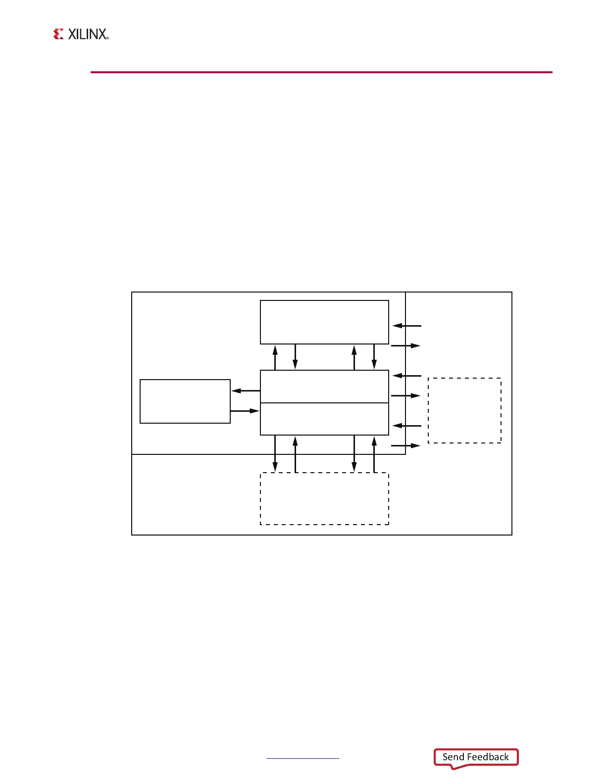
Zynq-7000 XC7Z045 AP SoC
[Figure 1-2, callout 1]
The ZC706 evaluation board is populated with the Zynq-7000 XC7Z045-2FFG900C AP SoC.
The XC7Z045 AP SoC consists of an integrated processing system (PS) and programmable
logic (PL), on a single die. The high-level block diagram is shown in Figure 1-3.
The PS integrates two ARM® Cortex™-A9 MPCore™ application processors, AMBA®
interconnect, internal memories, external memory interfaces, and peripherals including
USB, Ethernet, SPI, SD/SDIO,
I
2
C, CAN, UART, and GPIO. The PS runs independently of the PL
and boots at power-up or reset.
A system level block diagram is shown in Figure 1-4.
X-Ref Target - Figure 1-3
Figure 1-3: High-Level Block Diagram
Application
Processor Unit (APU)
Common
Peripherals
Custom
Peripherals
Common Accelerators
Custom Accelerators
Memory
Interfaces
Processing
System
(PS)
Programmable
Logic
(PL)
Input Output
Peripherals
(IOP)
High-Bandwidth
AMBA
®
AXI Interfaces
UG954_c1_03_100112
Interconnect

 Loading...


