ZC706 Evaluation Board User Guide www.xilinx.com 17
UG954 (v1.5) September 10, 2015
Feature Descriptions
I/O Voltage Rails
There are eleven I/O banks available on the XC7Z045 AP SoC. The voltages applied to the
XC7Z045 AP SoC I/O banks used by the ZC706 evaluation board are listed in Table 1-3.
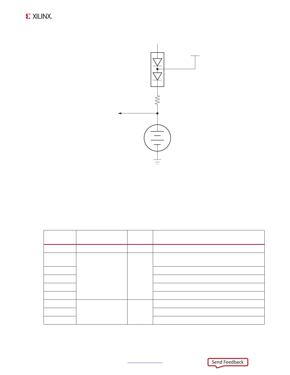
X-Ref Target - Figure 1-5
Figure 1-5: Encryption Key Backup Circuit
UG954_c1_05_041113
GND
2
1
B2
Lithium Battery
Seiko
TS518SE_FL35E
1.5V
2
1
3
BAS40-04
D7
40V
200 mW
NC
FPGA_VBATT
+
VCCAUX
R9
4.70K 1%
1/16W
To XC7Z045 AP SoC
U1 Pin P9
(VCCBATT)
Table 1-3: I/O Voltage Rails
XC7Z045 (U1)
Bank
Net Name Voltage Connected To
PL Bank 0 VCC3V3_FPGA 3.3V AP SoC Configuration Bank 0
PL Bank 9
VADJ_FPGA 2.5V
PMOD, USER_SMA_CLOCK, SM_FAN, REC_CLOCK,
SFP_TX_DISABLE
PL Bank 10 FMC_LPC, PL_JTAG,GPIO
PL Bank 11 FMC_HPC, GPIO_LED, HDMI
PL Bank 12 FMC_LPC, HDMI
PL Bank 13 FMC_HPC, HDMI
PL Bank 33
VCC1V5_PL 1.5V
PL_DDR3_D[31:0]
PL Bank 34 PL_DDR3_A, SYSCLK
PL Bank 35 PL_DDR3_D[63:32], XADC

 Loading...


