ZC706 Evaluation Board User Guide www.xilinx.com 44
UG954 (v1.5) September 10, 2015
Feature Descriptions
PCI Express Endpoint Connectivity
[Figure 1-2, callout 13]
The 4-lane PCI Express edge connector performs data transfers at the rate of 2.5 GT/s for a
Gen1 application and 5.0 GT/s for a Gen2 application. The PCIe transmit and receive signal
data paths have a characteristic impedance of 85Ω ±10%. The PCIe clock is routed as a
100Ω differential pair.
The XC7Z045-2FFG900C AP SoC (-2 speed grade) included with the ZC706 board supports
up to Gen2 x4.
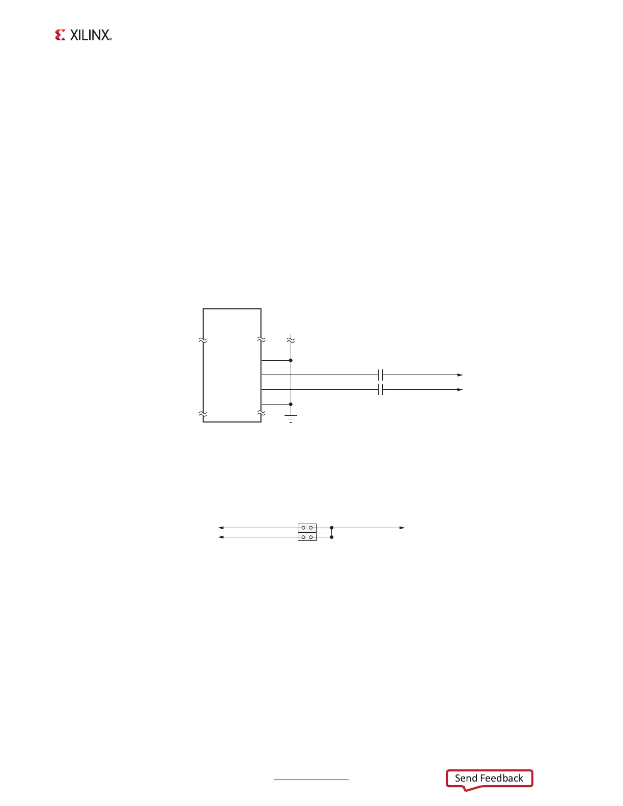
The PCIe clock is input from the edge connector. It is AC coupled to the AP SoC through the
MGTREFCLK0 pins of Quad 112. PCIE_CLK_Q0_P is connected to AP SoC U1 pin N8, and the
_N net is connected to pin N7. The PCI Express clock circuit is shown in Figure 1-17.
PCIe lane width/size is selected by jumper J19 (Figure 1-17). The default lane size selection
is 4-lane (J19 pins 3 and 4 jumpered).
X-Ref Target - Figure 1-17
Figure 1-17: PCI Express Clock
UG954_c1_17_041113
PCI Express
Eight-Lane
Edge connector
GND
GND
A15
A13
A14
P4
REFCLK+
A12
GND
C352
0.01μF 25V
X7R
C353
0.01μF 25V
X7R
PCIE_CLK_Q0_P
PCIE_CLK_Q0_N
PCIE_CLK_Q0_C_P
PCIE_CLK_Q0_C_N
OE
REFCLK-
X-Ref Target - Figure 1-18
Figure 1-18: PCI Express Lane Size Select Jumper J19
UG954_c1_18_041113
PCIE_PRSNT_BPCIE_PRSNT_X1
PCIE_PRSNT_X4
J19
1
3
2
4

 Loading...


