ZC706 Evaluation Board User Guide www.xilinx.com 43
UG954 (v1.5) September 10, 2015
Feature Descriptions
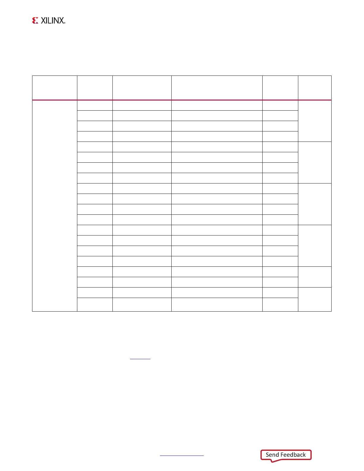
Table 1-15 lists the GTX Bank interface connections between the AP SoC U1 and FMC LPC
connector J5.
For additional information on Zynq-7000 GTX transceivers, see 7 Series FPGAs GTX/GTH
Transceivers User Guide (UG476
).
Table 1-15: AP SoC GTX Bank 111 Interface Connections to FMC LPC J5
Transceiver
Bank
AP SoC U1
Pin
Number
AP SoC U1 Pin
Name
Schematic Net Name
Connected
Pin
Connected
Device
GTX_BANK_11
1
AB2 MGTPTXP0_111 FMC_LPC_DP0_C2M_P C2
FMC LPC
J5
AB1 MGTPTXN0_111 FMC_LPC_DP0_C2M_N C3
AC4 MGTPRXP0_111 FMC_LPC_DP0_M2C_P C6
AC3 MGTPRXN0_111 FMC_LPC_DP0_M2C_N C7
Y2 MGTPTXP1_111 SMA_MGT_TX_P J35.1
GTX TX/RX
SMA
Y1 MGTPTXN1_111 SMA_MGT_TX_N J34.1
AB6 MGTPRXP1_111 SMA_MGT_RX_P
(2)
J32.1
AB5 MGTPRXN1_111 SMA_MGT_RX_N
(2)
J33.1
W4 MGTPTXP2_111 SFP_TX_P 18
SFP+
Conn. P2
W3 MGTPTXN2_111 SFP_TX_N 19
Y6 MGTPRXP2_111 SFP_RX_P 13
Y5 MGTPRXN2_111 SFP_RX_N 12
V2 MGTPTXP3_111 (capacitively coupled to AA4) U1.AA4
AP SoC U1
GTX
Loopback
V1 MGTPTXN3_111 (Cooperatively coupled to AA3) U1.AA3
AA4 MGTPRXP3_111 See Pin V2 loopback U1.V2
AA3 MGTPRXN3_111 See Pin V1 loopback U1.V1
U8 MGTREFCLK0P_111 FMC_LPC_GBTCLK0_M2C_C_P
(1)
D4
FMC LPC
J5
U7 MGTREFCLK0N_111 FMC_LPC_GBTCLK0_M2C_C_N
(1)
D5
W8 MGTREFCLK1P_111 SMA_MGT_REFCLK_P
(2)
J36.1 GTX
REFCLK
SMA
W7 MGTREFCLK1N_111 SMA_MGT_REFCLK_N
(2)
J31.1
Notes:
1. AP SoC U1 GTX input clock nets are capacitively coupled to the FMC LPC J5 pins.
2. AP SoC U1 GTX input nets are capacitively coupled to the RX and MGT_REFCLK SMA pins.

 Loading...


