ZC706 Evaluation Board User Guide www.xilinx.com 60
UG954 (v1.5) September 10, 2015
Feature Descriptions
GPIO DIP Switch
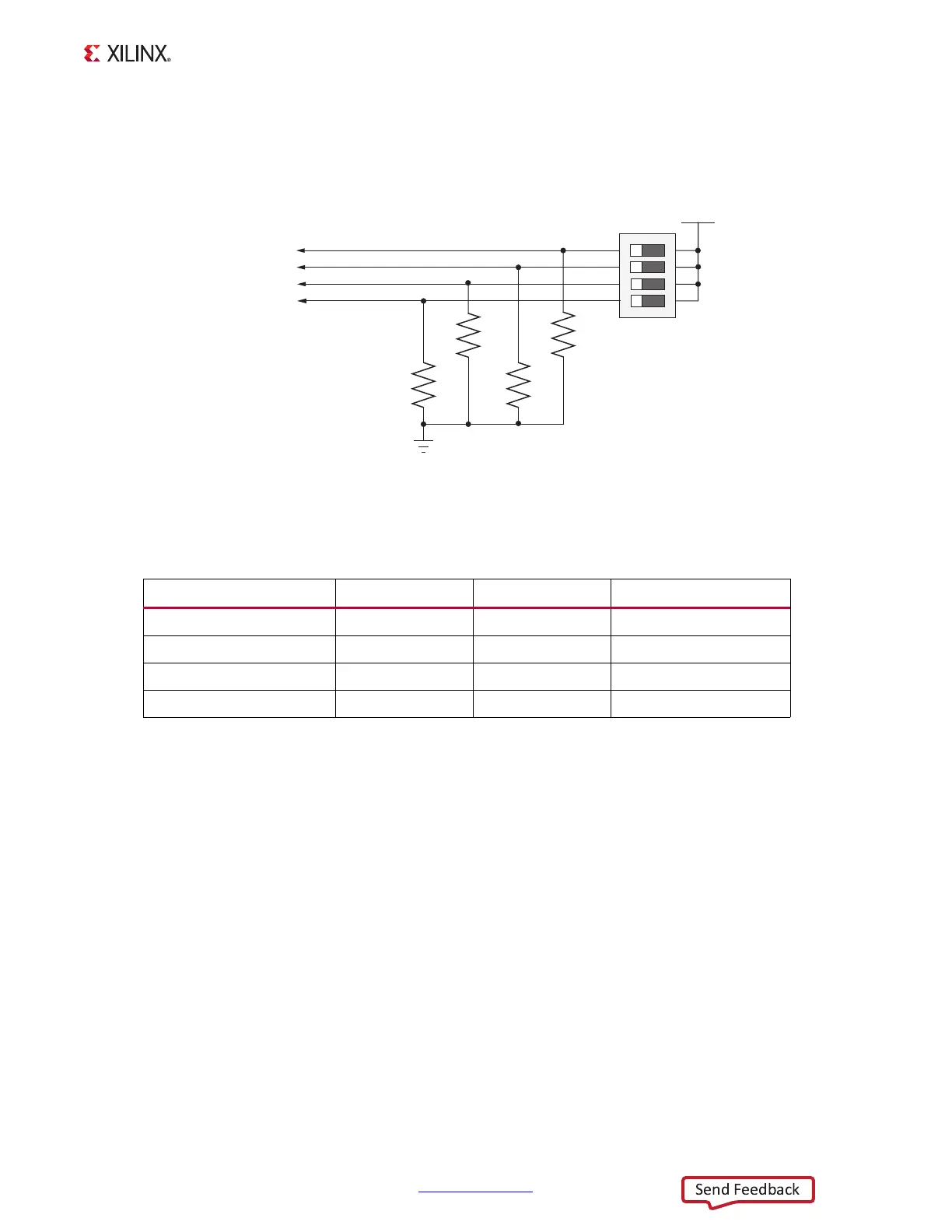
Figure 1-27 shows the GPIO DIP switch circuit.
Table 1-30 lists the GPIO DIP switch connections to XC7Z045 AP SoC U1.
User PMOD GPIO Headers
[Figure 1-2, callout 26]
The ZC706 evaluation board GPIO 2 x 6 male headers J57 and J58 support Digilent Pmod
Peripheral Modules. J57 pins (IIC_PMOD_[0:7]) are connected to the TI TCA6416APWR I2C
expansion port device U16. J58 pins (PMOD1_[0:7]) are connected to the TI TXS0108E
3.3V-to-VADJ level-shifter U40.
See the Digilent website for information on Digilent Pmod Peripheral Modules [Ref 35].
Information about the TCA641APWR and TXS0108E devices is available at the Texas
Instruments website [Ref 26].
X-Ref Target - Figure 1-27
Figure 1-27: GPIO DIP Switch
Table 1-30: GPIO DIP Switch Connections to XC7Z045 AP SoC at U1
XC7Z045 AP S0C (U1) Pin Net Name I/O Standard DIP Switch SW12 Pin
AB17 GPIO_DIP_SW0 LVCMOS25 1
AC16 GPIO_DIP_SW1 LVCMOS25 2
AC17 GPIO_DIP_SW2 LVCMOS25 3
AJ13 GPIO_DIP_SW3 LVCMOS25 4
UG954_c1_27_041113
SDA02H1SBD
SW12
VADJ
8
7
GPIO_DIP_SW0
GPIO_DIP_SW1
R70
4.7 kΩ
0.1 W
5%
R71
4.7 kΩ
0.1 W
5%
1
2
R68
4.7 kΩ
0.1 W
5%
R69
4.7 kΩ
0.1 W
5%
GND
GPIO_DIP_SW2
GPIO_DIP_SW3
6
5
3
4
1
2
1
2
1
2
1
2

 Loading...


