ZC706 Evaluation Board User Guide www.xilinx.com 53
UG954 (v1.5) September 10, 2015
Feature Descriptions
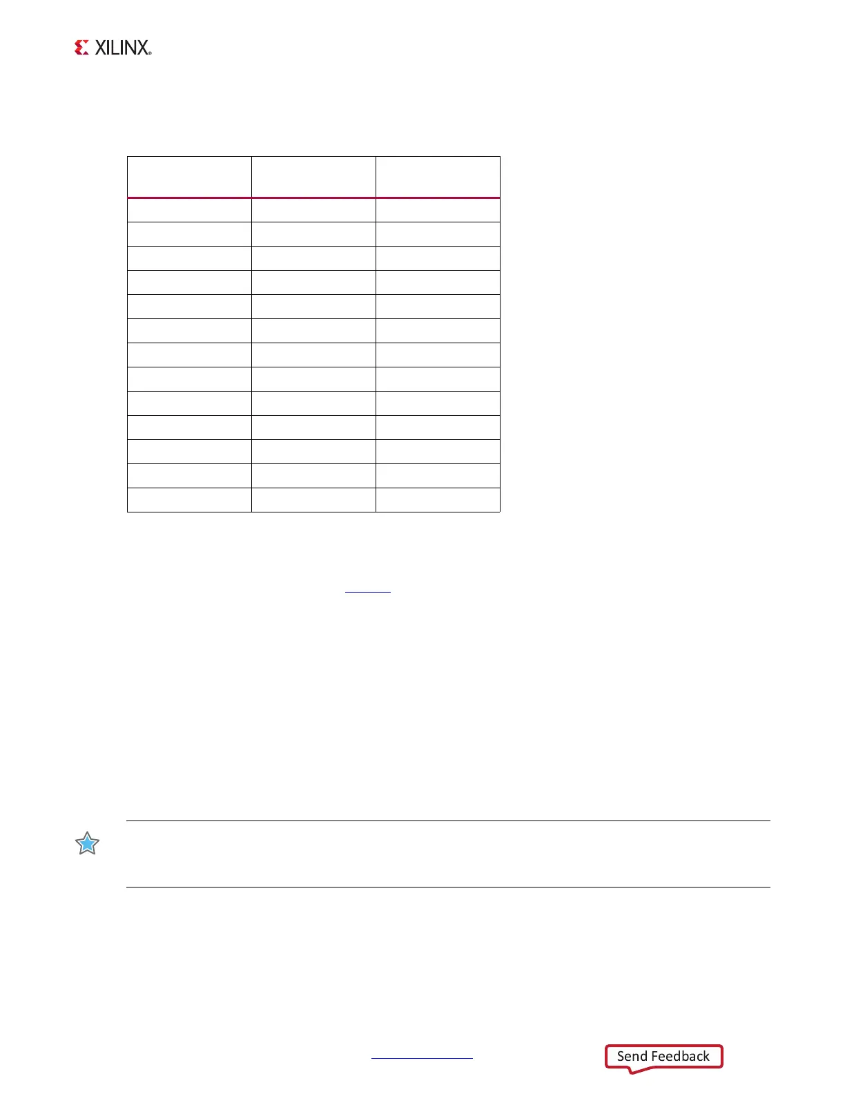
Table 1-24 lists the connections between the codec and the HDMI receptacle P1.
Information about the ADV7511KSTZ-P is available on the Analog Devices website [Ref 25].
For additional information about HDMI IP options, see the LogiCORE IP DisplayPort Product
Guide for Vivado Design Suite (PG064
).
I2C Bus
[Figure 1-2, callout 20]
The ZC706 evaluation board implements two
I
2
C ports on the XC7Z045 AP SoC. The PL-side
I
2
C port (IIC_SDA and _SCL_MAIN) is routed to level shifter U87. The PS-side I
2
C port
(PS_SDA and _SCL_MAIN) is routed to level shifter U88. The "output" side of the two level
shifters are wired to the common
I
2
C bus IIC_SDA and _SCL_MAIN which is connected to TI
Semiconductor PCA9548 1-to-8 channel
I
2
C bus switch (U65). The bus switch can operated
at speeds up to 400 kHz.
IMPORTANT: The PCA9548 U65 RESET_B pin 24 is connected to FPGA U1 bank 501 pin F20 via
level-shifter U25. FPGA pin F20 net IIC_MUX_RESET_B_LS must be driven High to enable I2C bus
transactions with the devices connected to U65.
Table 1-24: ADV7511 to HDMI Receptacle Connections
ADV7511 (U53) Net Name
HDMI Receptacle
P1 Pin
36 HDMI_D0_P 7
35 HDMI_D0_N 9
40 HDMI_D1_P 4
39 HDMI_D1_N 6
43 HDMI_D2_P 1
42 HDMI_D2_N 3
33 HDMI_CLK_P 10
32 HDMI_CLK_N 12
54 HDMI_DDCSDA 16
53 HDMI_DDCSCL 15
52 HDMI_HEAC_P 14
51 HDMI_HEAC_N 19
48 HDMI_CEC 13

 Loading...


