ZC706 Evaluation Board User Guide www.xilinx.com 54
UG954 (v1.5) September 10, 2015
Feature Descriptions
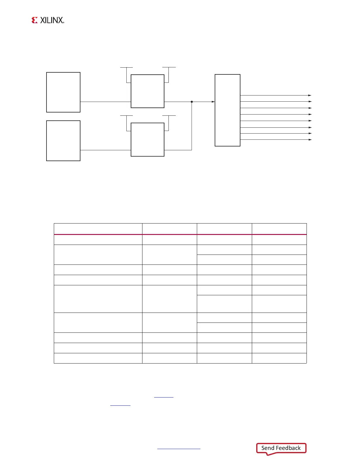
The ZC706 evaluation board I
2
C bus topology is shown in Figure 1-22.
User applications that communicate with devices on one of the downstream I
2
C buses must
first set up a path to the desired bus through the U65 bus switch at I
2
C address 0x74
(0b01110100). Table 1-25 lists the address for each bus.
Information about the PCA9548 is available on the TI Semiconductor website at [Ref 26].
For additional information on the Zynq-7000 AP SoC device I
2
C controller, see Zynq-7000
All Programmable SoC Overview (DS190
) and Zynq-7000 All Programmable SoC Technical
Reference Manual (UG585
).
X-Ref Target - Figure 1-22
Figure 1-22: I
2
C Bus Topology
CH7 - PMBUS_DATA/CLK
PCA9548
1
2
C 1-to-8
Bus Switch
U65
CH6 - FMC_LPC_IIC_SDA/SCL
CH5 - FMC_HPC_IIC_SDA/SCL
CH4 - IIC_RTC_SDA/SCL
CH3 - PORT_EXPANDER_SDA/SCL
CH2 - EEPROM_IIC_SDA/SCL
CH1 - IIC_SDA/SCL_HDMI
CH0 - USRCLK_SFP_SDA/SCL
XC7Z045 AP SoC
PS Bank 501
(1.8V)
U1
UG954_c1_22_04113
XC7Z045 AP SoC
PL Bank 10
(2.5V)
U1
PCA9517
I
2
C
Level Shifter
U87
3.3 V
VADJ 2.5V
AB
PCA9517
I
2
C
Level Shifter
U88
3.3 V
VCCMIO_PS 1.8V
AB
IIC_SDA/SCL_MAIN
PS_SDA/SCL_MAIN
IIC_SCL/SDA_MAIN
Table 1-25: I
2
C Bus Addresses
Device I
2
C Switch Position I
2
C Address Device
PCA9548 8-Channel bus switch NA
0b1110100 PCA9548 U65
Si570 clock 0
0b1011101 Si570 U37
0b1010000 SFP+ Conn. P2
ADV7511 HDMI 1
0b0111001 ADV7511 U53
I2C EEPROM 2
0b1010100 M24C08 U9
I2C port expander and
DDR3 SODIMM
3
0b0100001 Port Expander U16
0b1010000
0b0011000
DDR3 SODIMM J1
I2C real time clock and
Si5324 clock
4
0b1010001 RTC8564JE U26
0b1101000 SI5324 U60
FMC HPC 5
0bxxxxx00 FMC HPC J37
FMC LPC 6
0bxxxxx00 FMC LPC J5
UCD90120A pmbus 7
0b1100101 UCD90120A U48

 Loading...


