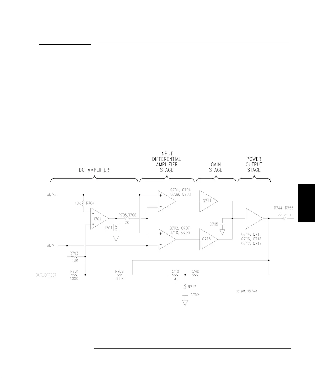
Output Amplifier
Block 7 on block diagram page 129; Schematic on page 137.
The output amplifier drives the function generator’s signal output
through the output attenuator section. The output amplifier exhibits an
approximate 35 MHz bandwidth and 1000 V/
ms slew rate. AC signals
originating from the DAC+ and DAC- signal paths are combined at the
input of the amplifier. The output amplifier exhibits a nominal x(-10)
voltage gain from its -AMP_IN input and a nominal x12 voltage gain
from its +AMP_IN input. A dc offset signal, related to the front panel
output offset value, is also summed with the ac signal at the input of the
amplifier. A simplified block diagram of the output amplifier is shown below.
5
Chapter 5 Theory of Operation
Output Amplifier
87
 Loading...