S9 Operator Board Maintenance Instructions
16
、
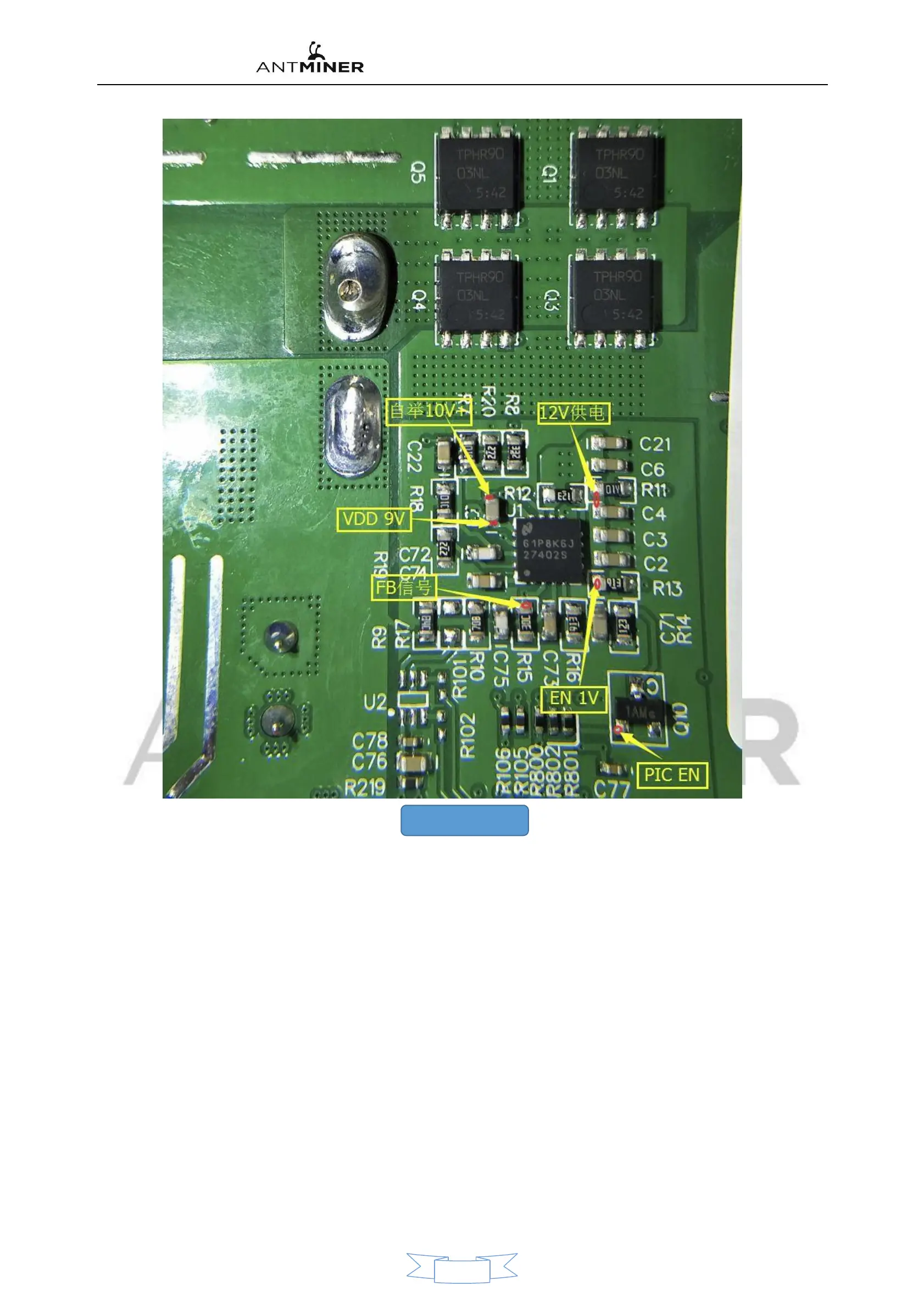
DC-DC Circuit
LM27402SQ Voltage Regulator Generation PWM Switching signals drive up and down bridges (Two pairs CMOS),and through L2
Inductor Energy Storage, Again by C19、C20 Filtering.
LM27402SQ Main function Pin
Pin 7 :12V Power supply,
Pin 9, 17:GND,
Pin 2 :FB Feedback Connection PIC Voltage determined by pin 8 of Pic to decide.
Pin 10 :Vdd
Pin 13 :Bootstrap capacitance 10v +
Pin 16 :Pulse
Pin 12 :Switching signal
Pin 11 :Lower Bridge Drive
Pin 14 :Upper Bridge Drive
DC-DC When the voltage is abnormal
,
First check through the fixture printing information to view PIC is the voltage value DC-DC is the output voltage one to
;
If
there is a disagreement between
,
Please change first
LM27402SQ The small capacitance around
;
If DC-DC No output
,
Please check R13
、
R14 Voltages 1v on both sides - R11 Voltage 12V
、
PIC Whether the work is abnormal, PIC Whether the control panel can
be accepted properly
I2C Signal.
DC-DC Output voltage Standard
:
14T Operation Board
:
8.3 V-8.6 V
13.5T Operation Board: 8.4 V-8.7 v
10
 Loading...