1, Test points 2, one of the voltage domains 3. IO 4. 14V Boost DC – PIC Control
9. 1.V – LDO 8. 25M CLK 7. 14V +B 6. DC +B
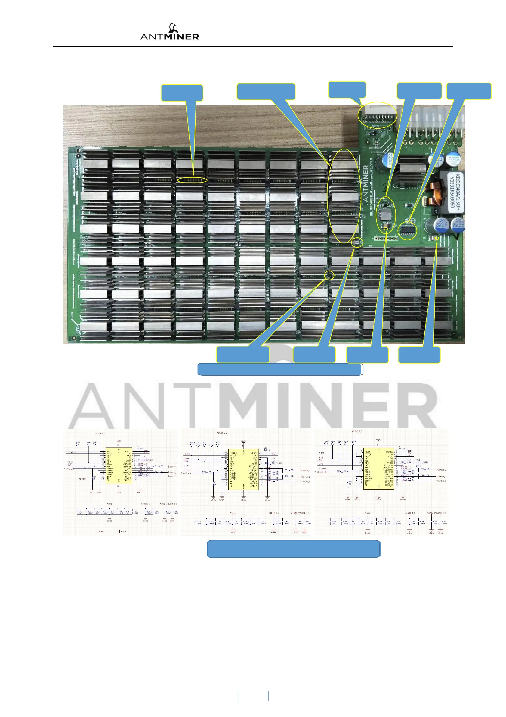
3、S9 Key circuits on the front of the Operation board
2) , voltage Domain:Full board has 21 Voltage domain,Each voltage has three chips. In the same voltage domain. 3 A chip to power the
associated power supply,The correlation is then concatenated with the other voltage domains. Circuit structure such as
The following figure 4 is
shown
:
图 4、S9 Key circuits on the front of the Operation board
Note that:
Because the version of the S9 computing board is not exactly the same, the LDO-1.8V power supply of the early voltage domains is powered by a separate peripheral
LOD power supply chip for each of the three voltage domains. The later version is changed to the internal chip. Power supply (BM1387 chip with 2.5 V input, 1.8 V
output LDO supply circuit), except for the last six voltage domains, which are powered by 14V boost and LDO externally, all other chips provide LDO1.8V power
supply, while PLL -0.8V is obtained by dividing the first chip LDO -1.8V in each voltage domain by a voltage divider resistor (late version)
3
 Loading...