Operator Board Maintenance Instructions
Need to be aware of:An abnormally high voltage rise in the boost circuit can lead to the calculation board finally 6 Voltage domain. LDO
Damage,also easily lead to chip damage. While the boost voltage
the exception is mostly U110
、
R812
、
R811 Oxidation-induced.
5
、
DC-PIC
:
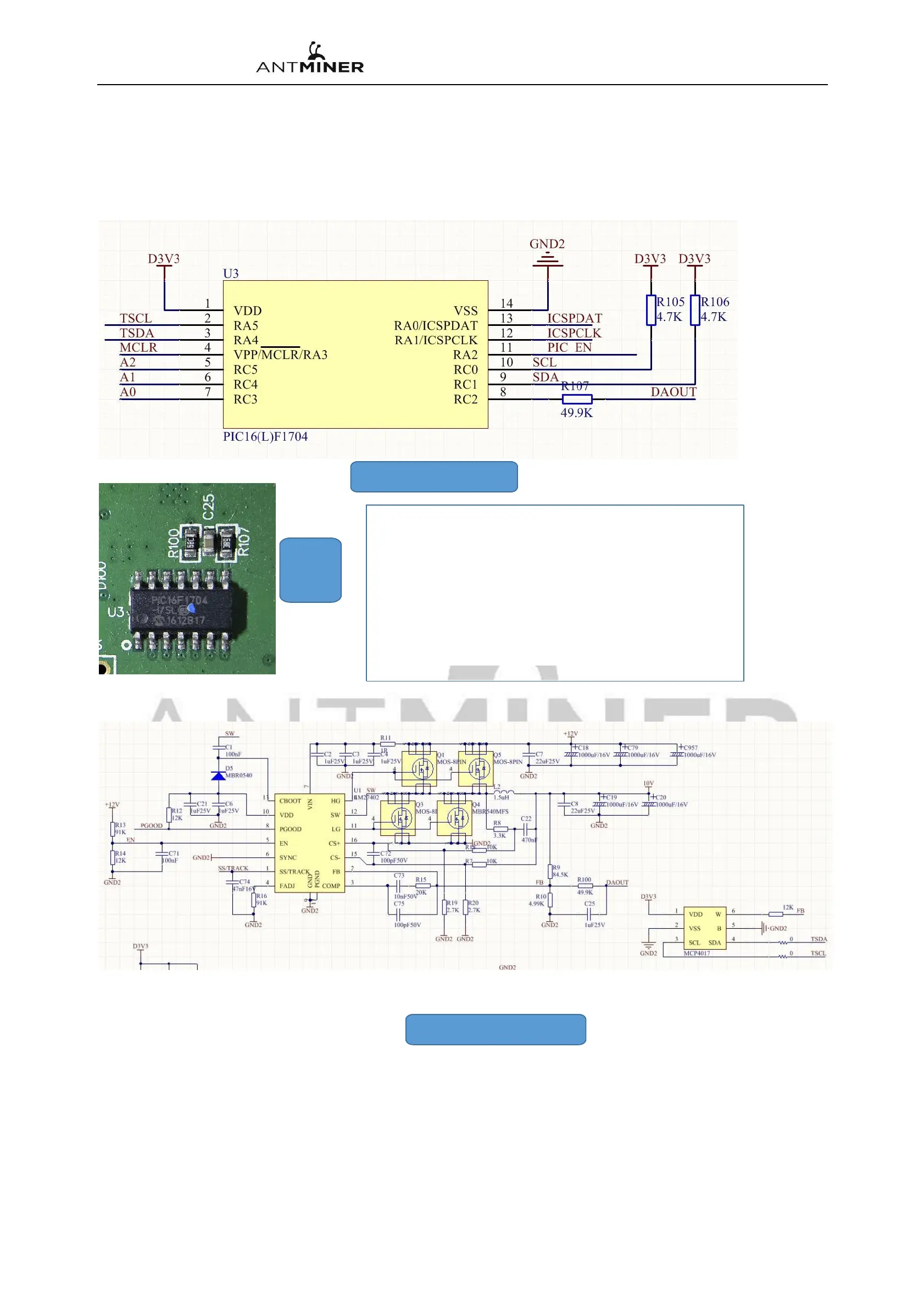
PIC16 (L) F1704 Composition As shown in figure 13 and Figure 14
:
A device that stores the frequency information and voltage values of an operational board chip,It also allows control of the operational DC-DC Output voltage.
13、PIC Schematic diagram
14、
PIC
6
、
DC-DC Circuit
:由
LM27402SQ
与
CMOS
管
TPHR9003NL Composition Figure 15 below and Figure 16 is shown
:
15
、
DC-DC Schematic diagram
9
PIC is running, every minute, we need to control the heartbeat signal.,if
not, With heartbeat information, PIC will work for one minute and then
shut down.
PIC pin 1 is VDD 3.3V, 14 is GND, pins 9 and 10 are connected to the I2C
bus of the IO port to the control board, pins 5, 6, and 7 are PIC addresses;
pin 4 is PIC3 .3V; pin 8 is PIC.
FB output, control DC-DC voltage; 11 pin is EN signal of PIC output, control
DC-DC working status.
Figure 15
 Loading...