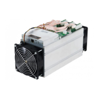
S9 Operator Board Maintenance Instructions
5, Broken chain
;
A broken chain is like a missing chip.,But the broken chain is not the chip to find the core is abnormal,Instead, all the chips on the back
of the abnormal chip fail because of an abnormal chip. Like a chip book.
I can work.
,
But it does not forward other chip information
;
Then
,
The
entire signal chain will come to an abrupt halt here.
,
Lose a large part of
,
is broken chain.
Broken chain general test box can be displayed,Like
what:When the test box detects the chip,,Only detected 14 A chip,If the preset number of chips is not detected in the test box It's not
working.,So it only shows how many chips are detected.,At this point, only the numbers displayed“14”,In section 14 Detect the voltage
and impedance of each test point before and after a chip can find a problem Area
6, do not run
;
Do not run means that the test box does not detect the chip information of the Operation board,and display NO hash board;This phenomenon is most
common,The range of faults involved is also wide. 1), a voltage-domain voltage anomaly caused by the non-operation;The problem can be identified by
measuring the voltages in each voltage domain.
2), an abnormal chip caused Anomalies can be found by measuring each test point signal. CLK Signal:0.9 in;Signal by 00 Number of chips output to 62
Number Chip,But the current version is only one crystal oscillator,Where the signal is abnormal. LCK 的,All the signals in the back are abnormal.,根 The signal is
transmitted in the order of direction lookup.
TX Signal
:
1.8 in
;
This signal is determined by the 00
、
01
、、、、、、
62 Number of chips
,
When the dichotomy of a point anomaly, forward detection can be.
RX Signal
:
1.8 in
;
This signal is determined by the 62
、、、、、、
01
、
00 Number returned by the
,
Identify the cause of the fault through chip signal direction
,
S7
和
S9
运
The
board does not run the signal as the highest priority
,
First find the signal.
BO Signal:0V,The signal is detected on the chip Re When the signal returns to normal,To be pulled down to high level,Otherwise the high level.
RST Signal
:
1.8 in
;
Power on the operational board and plug it in I After the signal
,
This signal will be 00
、
01
、、、、、、
62 Direction to the last chip. 3
)
A chip Vdd Caused by
Can be measured by measuring the potential difference in each voltage domain is normal,Under normal circumstances,当 Vdd Voltage is 0.4 in 时,The
normal voltages for each test point in other voltage domains are also 0.4 in,To ensure that each electric
Balance between the pressure domains.
4)of a chip. VDD1V8 Voltage anomalies
By measuring the test points of each voltage to determine VDD1V8 Voltage is normal,Under normal circumstances,I Voltage
Determines the voltage at each test point,当 I Voltage is 1.8 in 时,All test points in other voltage domains are normally electrically
Pressure also for 1.8 in
5)of a chip. VDD2V5 Voltage anomalies
Confirm the voltage is normal,Not normal with Vdd Voltage is relatively low. 6)The step-down circuit and the boost circuit are caused by
abnormal
Direct measurement of the upper left corner of the operation board C8 Capacitance output Are the voltages on both sides 8.27-9.07 in
Between,No or more than needed to U3 PIC Re-upgrade;Confirm PIC After the voltage is normal,检 测 U100 Whether there is output
15V Voltage ,Non-detectable peripheral parts and U100 Itself.
7Low
;
Low calculation capacity can be divided into
:
1) When testing a box test,The box received the Nuncio Enough,Not enough power to show in the。This phenomenon can be
directly through the test box of the serial printing information to see the return of each chip
Nence The quantity is judged by how much,General return Nence The number of chips below the set value should be
troubleshooting,Excluding non-false solder,Outside reason,The chip can be replaced directly.
2) When testing a box test,But after the machine installed, the calculation force is low.Most of this is related to the cooling conditions of the
chip.,Need to pay special attention to each chip of the small heat sink with glue,and the whole
The ventilation performance of the machine. Another reason is that a chip's voltage is at a critical,After loading the machine,12V Power
supply and test power supply differences cause the test and operation of the calculation force is biased,可
Test with test box after lowering,Slightly adjustable voltage DC The Adjustable power supply 12V After output,To test again,Find the
return Nence The lowest number of voltage domains are all chip to troubleshoot. 8, a Chip in the;
When passing test box testing,Test box serial port information shows the return of a chip Nence Insufficient or zero,In addition to the
problem of solder and peripheral components,The chip can be replaced directly.
●Maintenance Instructions:
1, maintenance,The service technician must be familiar with the function and flow direction of each test point, the normal voltage value and the
impedance value of the ground. 2, must be familiar with chip welding,To avoid causing PCB Blistering deformation or pin damage.
3、bm1387 Chip encapsulation,Chip on both sides 16 Feet. Polarity and coordinates must be aligned when soldering,cannot be misplaced.
4, when replacing the chip,Must clean the heat conduction fixing glue around the chip,Lest IC The chip is damaged two times when it is not floating or cooling
properly during welding.
● Precautions:
1.Because the back of the chip is connected to the chip,Special slender pen must be used to detect test point signals,And the stylus is exposed to metal except the
contact tip.,Other places must be used Heat shrinkable tube Sealing off insulation,In order to avoid the test point,The stylus is exposed to both the heatsink and
the test point. The voltage difference between the two-row circuit is very large.,Simultaneous exposure to different voltage domains(散
Hot film
)
And the test point
would create a man-made damage chip.
,
Special attention.
2.Welding,Because the back of the chip is tightly attached PCB Plate of the small heat sink,Heat conduction is faster. So in the welding must need to use the bottom
auxiliary heating(200 degree or so),can improve efficiency and reduce the PCB Damage to the board. If there is no bottom heating device,When replacing the
chip,The back of the chip must first be PCB The small heatsink on the board is taken down and replaced.
!
New fault type please contact our engineering department in time,We will continue to analyze and update this content!
20
 Loading...