The XILINX control panel is restored to the factory setting. In the shutdown state, press and hold the IP Report button for more than 5 seconds, then release it and start the
recovery.
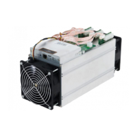
Iv. Routine Maintenance process
:
● Reference steps:
Observe the appearance Locate the chip, Reposition
Measuring impedance
Measurement voltage
System Tools Testing each test point
Test Voltage and power supply
Ok After the related aging
Based on Resolder Chip into place
the detection
information
Locate
faults
Make a good fault Test if Above good
Record Then Ok To be repaired.
1
、
Routine inspection
:
First of all
,
take a visual on the Repair board first, See if there is a small heat sink shift
,
Deformation
,
The phenomenon of burning
coke
?
If there is a need to deal with
;
The small heat sinks shifts
,先
After the demolition, Wash away the original gum
,
Repair and re-glue after passing.
Secondly,after visual inspection, no problem.,The impedance of each voltage domain can be detected first,detects if there is a short circuit, or open
circuit condition. If there is any discovery,must be handled well.
Again,Detection of voltage in each voltage domain is achieved 0.4v, The voltage difference of each voltage domain must not exceed 0.05。 A voltage field
voltage is too high or too low,the circuit of its adjacent voltage field is usually stored In abnormal phenomena. You need to troubleshoot the cause first.
2、 After routine testing, no problem. (Short-circuit detection of general routine testing is a must, Avoid burning chips or other materials due to short circuits when
energized),Chip detection with test boxes available,And according to
Test box detection results to determine positioning.
3、 Display results based on test box detection,Start near the faulty chip,Detection chip test point(CLK IN OUT/TX IN OUT/RX IN OUT/B IN OUT/RST IN OUT)
VDD VDD 0V8 VDD 1V8 VDD 2V5 Equal voltage.
4
、
And then according to the signal flow apart RX Signal Reverse Transfer
(
63
到
1 Number Chip
),
Several of these signals CLK CO BO RST For forward
delivery
(
1-63
),
Finding abnormal faults by power supply sequence
Point.
5、 When locating to a faulty chip,The chip must be re-welded. The method is to add flux around the chip(Preferably a no-wash flux),Heating the solder points
of the chip pin to a dissolved state, Move lightly under the left and right,Press the Chip;Enable the chip pin to be re-enchanted with the pad,Collect tin. To achieve
the effect of re-tin. If you re-weld,,The fault is still the same,The chip can be replaced directly.
6、 After repairing the operation board,When testing box detection,Must be more than two times. Two test times before and after:First time,After
the replacement parts have been completed,Requires the operation board to cool down,Pass the test
After passing,Put one side first. Second time,After a few minutes, the arithmetic board cools completely.,To test again. Although the two tests have a
few minutes to be spent,,But this does not affect the work. will be repaired
Board on one side.,Keep repairing the second board.,And wait for the second plate to be repaired and cooled.,Test the first block again. So time just
staggered,Did not delay the total length of time.
7、 The repaired board. Need to classify the fault,and the replacement component model, location, reasons and other aspects of the record. For feedback
back to production, after sale, research and development.
8、 After the record.,Re-installed into the whole machine for normal testing.
Fault type:
S9 Common fault types are:
1、 Heat sink, heatsink shift, variant; Not allowed on the back of the board chip before powering on PCB Heatsink displacement on the board,Have
collided,In particular, different voltages of the heatsink. Different voltage domains The heat sink is exposed to the possibility that a different voltage point will
be shorted. And make sure each heatsink on the op-amp has a good heat conduction.,Fixed firmly. Replace or re-heat the heatsink,It is necessary to clean the
heat sink, the residue on the chip and then re-glue the adhesive.,Residual heat conductive adhesive can be cleaned with anhydrous alcohol.
2、 Impedance imbalance in each voltage domain; When the impedance of some voltage domains deviates from normal,It is indicated that there are open
circuit and short circuit in abnormal voltage domain. The general chip is the most likely cause
Big. But there are three chips per voltage domain.,Often fail when,Only one of the problems. The method of finding out the problem chip can detect the anomaly
of the ground impedance by the test point of each chip. Point. If you encounter a short-circuit phenomenon,The same voltage can be first removed from the heatsink
on the chip,Then observe the chip pin has no tin phenomenon. If the appearance cannot find a short-circuit point,The short-circuit point can be found according to the
resistance method or current interception method.
3, voltage-Domain voltage imbalance;
When some voltage field voltages are too high or too low,In general, its abnormal voltage domain or adjacent voltage domain exists I Case of abnormal
signal,Cause one or the next voltage field to work in an abnormal state and the voltage imbalance. The anomaly can be found by detecting the signal and
voltage at each test point.,The individual needs to find the anomaly by comparing the impedance of each test point. Pay special attention to,CLK Signal and RST
Signal,These two anomalies are the most likely to cause voltage imbalance.
4, missing chips; Missing chip is the test box at the time of detection,Not all of them are detected. 63 A chip,Often only the actual number of chips is not
detected. and the actual missing(Not detected) The exception chip is not in the displayed position,In this case, the abnormal chip should be accurately located by
testing. The positioning method can be used TX By the way of the deadline issued,Find the location of the abnormal chip. is to put a chip's TX Signal to ground,For
example:The first 50 A chip. TX The output of the field to the voltage domain After,Theoretically, if all the chips in front are normal, ,The test box should show the
detected 50 A chip?If you do not detect 50 A chip,Description exception in 50 A chip before;如 The fruit detects 50 A chip,Description of the abnormal chip in the
first 50 After a chip. The second method is used to find out the location of the anomaly chip.
19
 Loading...