S9 Operator Board Maintenance Instructions
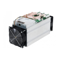
10、IO The signal is divided into piezoelectric
4
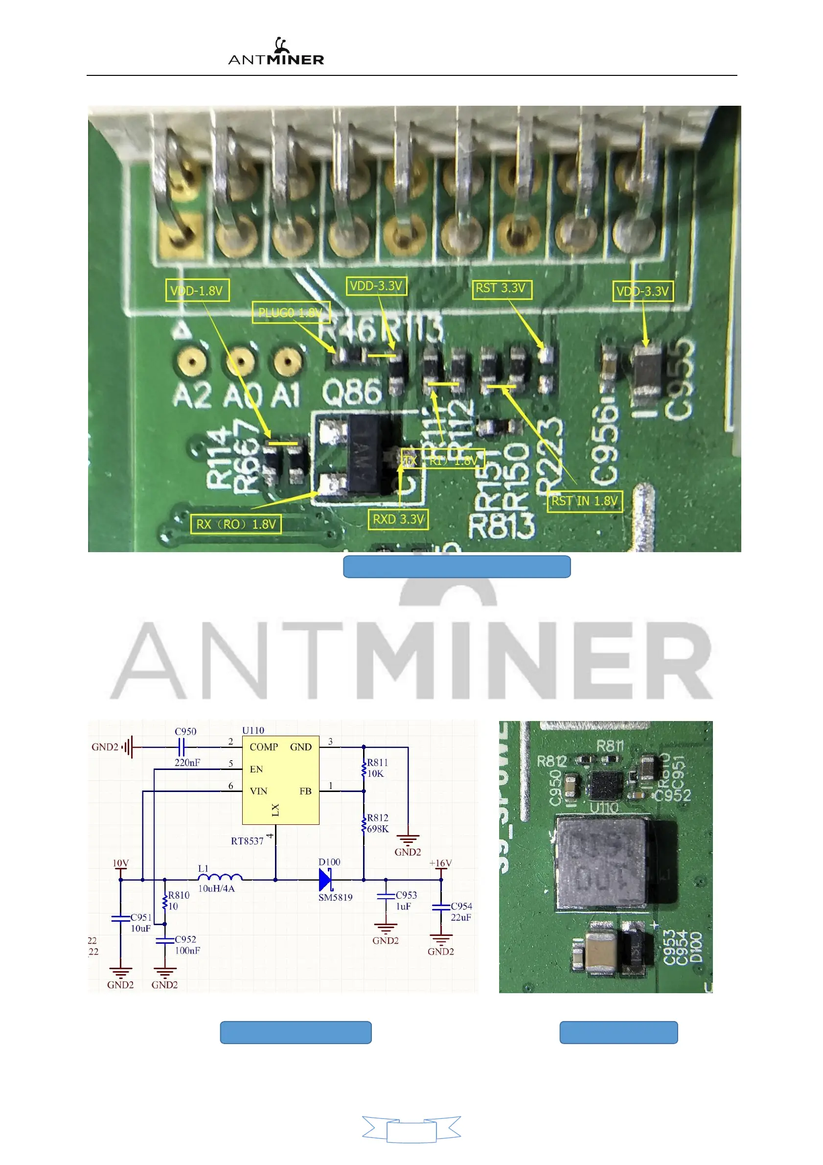
、
14V Boost circuit
:
Responsible for the DC-DC
(
8.3 — 9.2 V
)
Boost to 14V
,
The principle is through U110 (RT8537) The switching power supply will boost 9v to 14 V
,
The
switching signal produced by U110 passes the output switch signal through L1
The switching signal produced by U110 passes the output switch signal through
L1 for storage. can inductance, inductor, a boost rectifier diode D100 and then C954 to charge and discharge, whereby the discharge, to thereby obtain a
positive electrode C954 of 14 V
。
As shown in figure 11Figure 12 is shown
:
11
、
14V Boost schematic diagram
12
、
14V Boost PCB
8
 Loading...