●Key point Analysis:
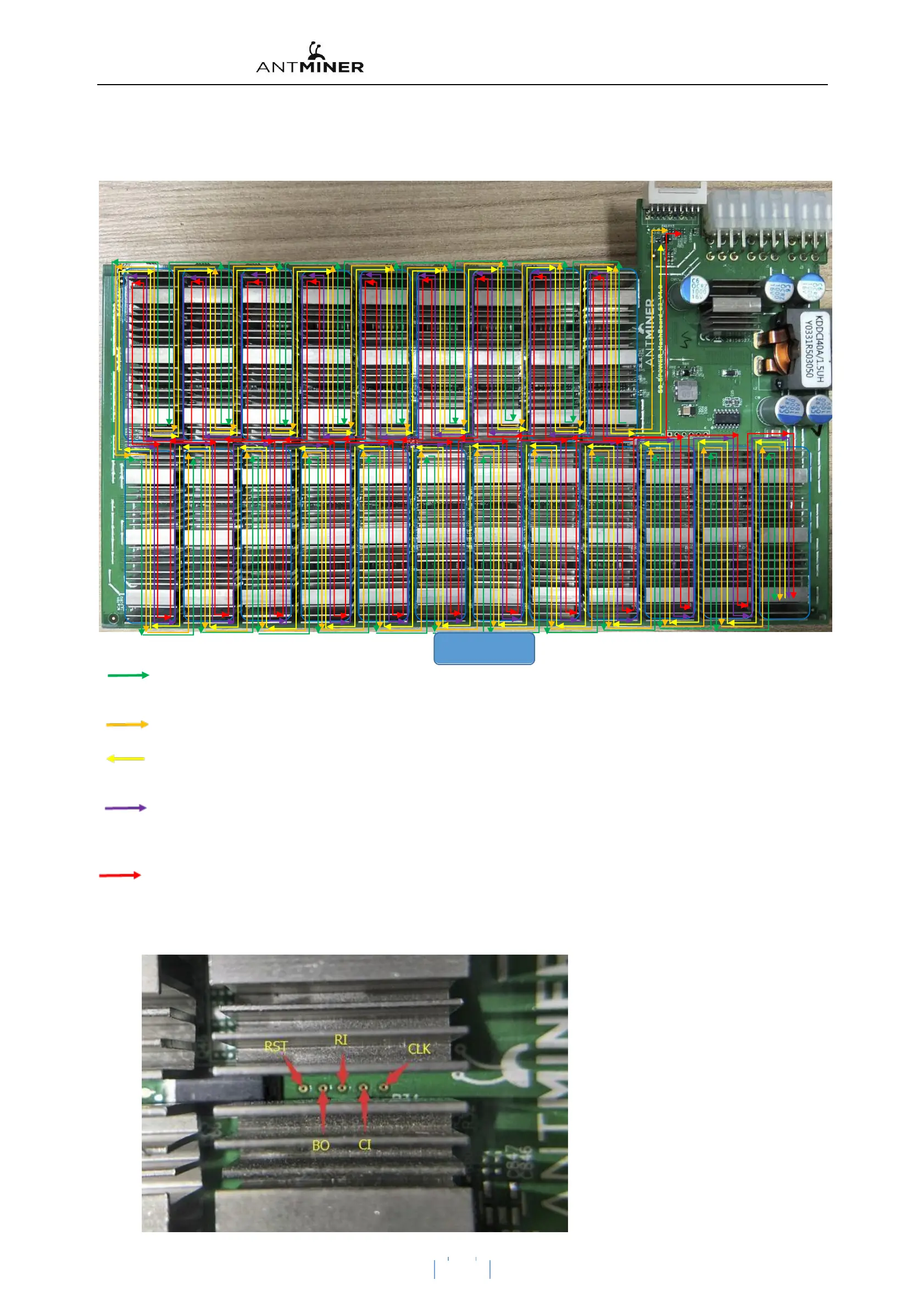
1、 The following figure is S9 Schematic diagram of signal board signal direction:
1
26
23
20
17
14
11
08
05
02
25
22
19
16
13
10
07
04
01
24
21
18
15
12
09
06
03
00
27
30
33
36
39
42
45
48
51
54
57
60
28
31
34
37
40
43
46
49
52
55
58
61
29
32
35
38
41
44
47
50
53
56
59
62
1, Signal direction
Green is the flow direction of the CLK signal, from the signal flow direction, from the signal flow direction, generated by the Y1
25M crystal oscillator, from the generation, from the 00 chip to the chip to the 62 chip transfer chip transmission; standby; standby and
operation, electricity and operation, electricity When the operation is performed
Orange is the signal flow direction of TX (CI, CO) signal. It enters from IO port 1 and then enters, and then transmits from chip No. 00 to chip
to chip 62. When the voltage is line is not inserted, the voltage is 0. The voltage at the time of operation is 1.8V.
。
yellow is the RX (RI, RO) signal flow direction, and the chip returns from the chip No. 62 to the chip No. 00, and then returns to
the control return board from the IO port 12 pin. When the IO signal is not inserted, the voltage is the voltage at the time of 1.8V. When
the operation is performed, the voltage is also 1.8V when the operation is performed.
Purple for B(BI、BO)Signal Flow,由 00 Number chip toward 62 Pull Low Level;Not plugged in. I Line, Standby time is
0V,When the operation is 0.3 Around the pulse signal. Purple is B (BI, BO) signal flow, ) signal flow, from 00 chip to chip to 62 low level;
no low level; no low level; no low level; no IO line It is 0V during standby, and is a pulse signal of about 0.3 at the time of calculation. Pulse
signal.
Red is the flow direction of RST signal, signal flow direction, signal flow direction, from IO port 15 foot, then from, then from,
then from 00 chip to 62 chip transfer chip transmission chip transmission; no IO signal, standby It is 0V during standby, and is calculated
during operation. It is 1.8V when calculating.
2. Figure 3 shows the key circuits on the front of the S9 computing board.
1
)
, test points between each chip
(
After zooming in the image
below
):图
2
During maintenance
,
the test point between the test chip is the
most straight
The fault location mode of the connection. S9
Operational Board test pilot
Row listed as
:
Upper Row 9 Sequencing of voltage domains
:
RST
、
B0
、
RI
(
RX
)、
C0
(
TX
)、
CLK Signal.
Bottom row 12 The order in which the voltage domains are arranged
in turn
:
CLK
、
CO
(
TX
)、
RI
(
RX
)、
BO
、
RST
。
图 2, inter-chip test points
2
 Loading...