S9 Operator Board Maintenance Instructions
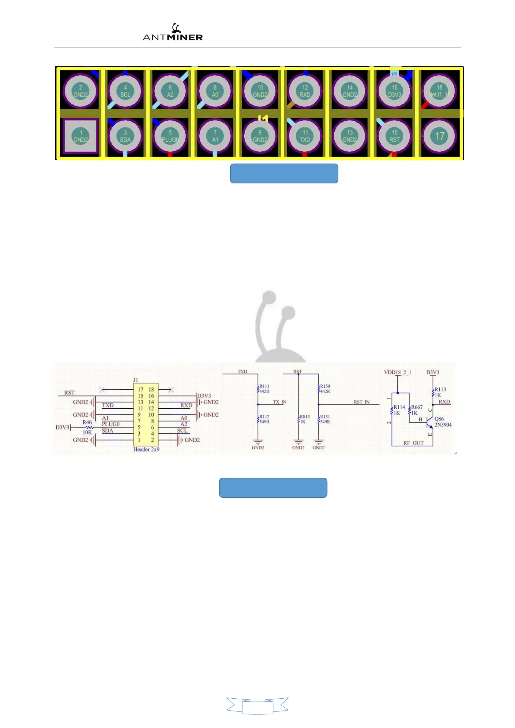
8. IO Pin definition for each port
As shown in the figure above
:
1
、
2
、
9
、
10
、
13
、
14
:
GND
。
3
、
4
(
SDA
、
SCL
):
DC-DC PIC I2C Bus
,
Connect the Control Panel to PIC of communication
,
The control board can read and write through it PIC
Data
,
Control the operating state of
its operational board.
5 (PLUG0
):
Identifying signals for the operating board
,
This signal is pulled by the operator board. 10K Resistance to 3.3 in
,
So plug it in. I Signal when
,
The foot should be
to high level.
6
、
7
、
8
(
A2
、
A1
、
A0
):
PIC Address signal.
11
、
12
(
Txd
、
RXD
):
For the arithmetic board 3.3 End of the counting force of the channel
,
After being divided by a resistor, it becomes TX
(
CO
)、
RX
(
RI
)
Signal
,
I Port pin End ping du for 3.3v
,
After the voltage is divided by the resistor
,
Become a 1.8v.
15
(
RST
):
To reset the signal 3.3v
,
After being divided by the resistor, it becomes 1.8v in RST Reset Signal.
16
(
D3V3
):
For the arithmetic board 3.3v Power supply
,
3.3v Provided by the Control Panel
,
Mainly to the PIC provides operating voltage.
Figure 9 , Figure 10 are shown as IO Voltage and distribution of each pin before and after the pressure is divided.
9、I Each voltage of the signal
7
 Loading...