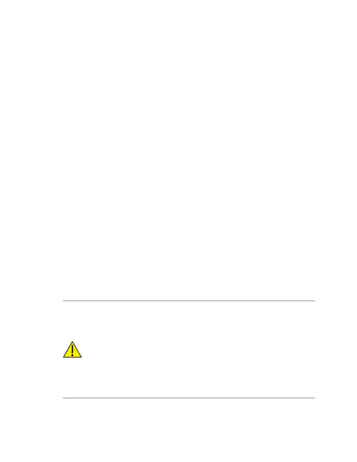
About the module Module pinout
ConnectCore for i.MX51 Hardware Reference Manual
13
Module pinout
The module has two 180-pin connectors, J1 and J2. The following tables describe each pin, its
properties, and its use on the module and development board. The DC parameters for each I/O type
are defined in the I/O DC parameters.
The “Use on module” column shows the connection of the signals on the module. The format of this
column is “component: pad_name,” where “component” is the chip where the signals are connected,
and “pad_name” is the name of the pad where the signals are connected as they are defined in the
component’s datasheet.
Pinout legend
I Input
O Output
IO Input or output
P Power
# Low level active signal
Pinout definitions
GPIO - General Purpose IO
UHVIO - Ultra High Voltage IO
HSGPIO - High Speed GPIO
LVIO - Low Voltage IO (meaning 1.8V)
The I/O Type descriptions can be read as follows:
n 18 - 1.8V logic level switching (for example, GPIO18)
n 27 - 2.775V logic level switching (for example, GPIO27)
n 31 - 3.15V logic level switching (for example, UHVIO31)
n 33 - 3.3V logic level switching (for example, UHVIO33)
The microprocessor used on this module, like all CMOS devices, can be driven into a latch-
up condition if any I/O pin is driven outside of its associated power rail. Care must be taken
to:
n Never drive an I/O pin beyond its positive rail or below ground.
n Never drive an I/O pin from an external power source during the power-on or reset
sequences.
n Never hot-swap the module or interrupt its ground connection to external circuitry.
Latch-up is a condition that can cause excessive current draw and result in excessive
heating of the microprocessor or its power supplies. This excessive heating can
permanently damage the microprocessor and/or its supporting components.