A-7
Appendices
NJ-series CPU Unit Hardware User’s Manual (W500)
A-2 Specifications of Basic I/O Units
A
A-2-2 Basic I/O Units
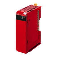
CJ1W-ID212 DC Input Unit (24 VDC, 16 Points)
*1 The ON response time will be 15 s maximum and OFF response time will be 90 s maximum even if the response time
are set to 0 ms due to internal element delays.
*2 Terminal numbers A0 to A8 and B0 to B8 are used in the external connection and terminal-device variable diagrams.
They are not printed on the Units.
Name 16-point DC Input Unit with Terminal Block
Model CJ1W-ID212
Rated Input Voltage 24 VDC
Allowable Input Voltage Range 20.4 to 26.4 VDC
Input Impedance 3.3 k
Input Current 7 mA typical (at 24 VDC)
ON Voltage/ON Current 14.4 VDC min./3 mA min.
OFF Voltage/OFF Current 5 VDC max./1 mA max.
ON Response Time
8.0 ms max. (Can be set to between 0 and 32 ms in the Unit Information settings.)
*1
OFF Response Time
8.0 ms max. (Can be set to between 0 and 32 ms in the Unit Information settings.)
*1
Number of Circuits 16 (16 points/common, 1 circuit)
Number of Simultaneously ON
Points
100% simultaneously ON (at 24 VDC)
(Refer to the following illustration.)
Insulation Resistance 20 M between external terminals and the GR terminal (100 VDC)
Dielectric Strength
1,000 VAC between the external terminals and the GR terminal for 1 minute at a leakage current of 10
mA max.
Internal Current Consumption 130 mA max.
Weight 110 g max.
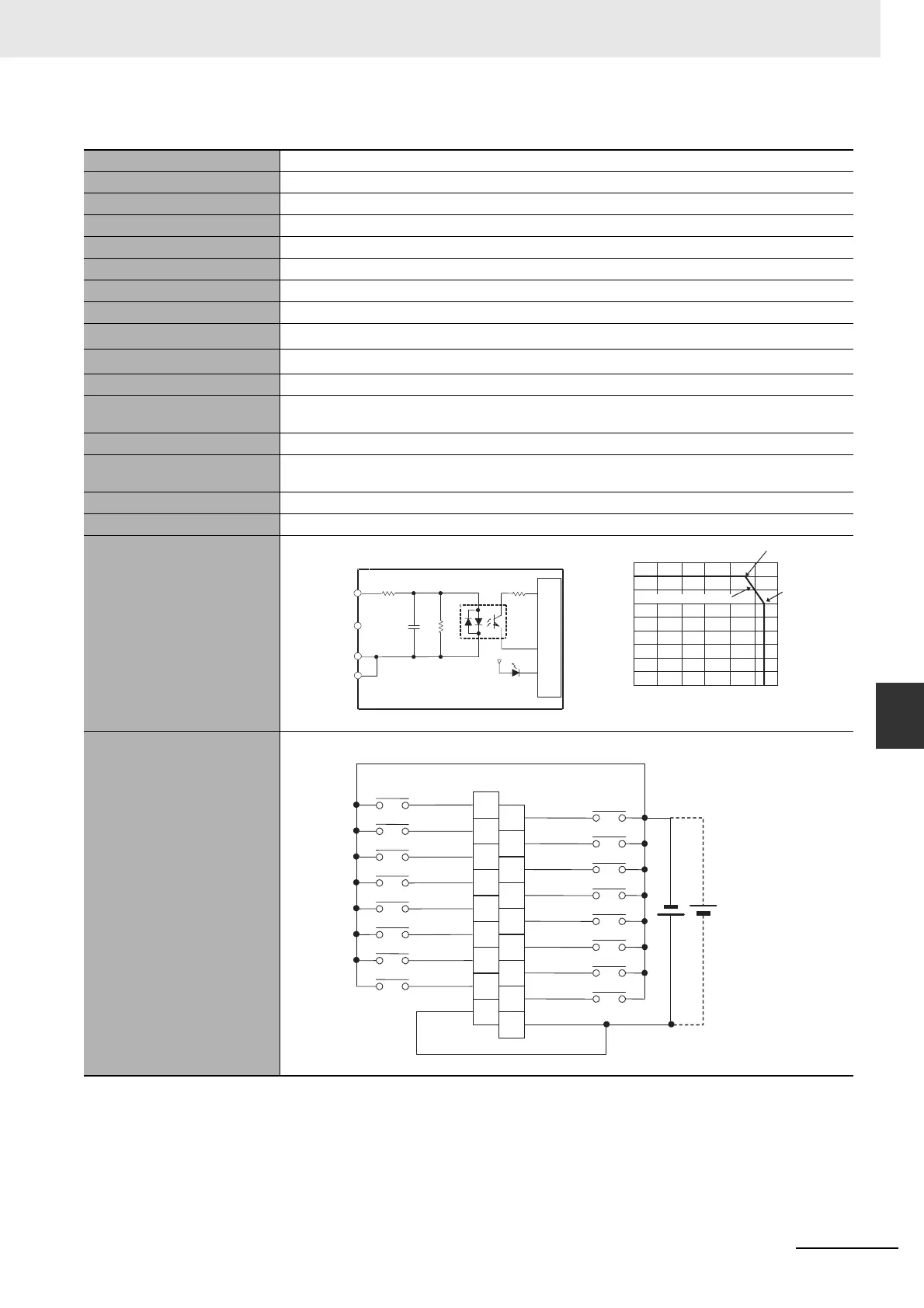
Circuit Configuration
External connection and termi-
nal-device variable diagram
• Polarity of the input power supply can be connected in either direction.
1000 pF
470
Ω
3.3 k
Ω
Internal circuits
Input indicator
to
Signal
name
Jxx_Ch1_In00
Jxx_Ch1_In15
COM
COM
18
16
14
12
10
8
6
4
2
0
0 10 20 30 40 50 60
No. of simultaneously ON points
Input voltage: 26.4 VDC
12 points
at 55°C.
16 points
at 45°C.
Ambient temperature
(°C)
Temperature characteristics
for simultaneously ON points
B1
Jxx_Ch1_In01
B2
Jxx_Ch1_In03
B3
Jxx_Ch1_In05
B4
Jxx_Ch1_In07
B5
Jxx_Ch1_In09
B6
Jxx_Ch1_In11
B7
Jxx_Ch1_In13
B8
Jxx_Ch1_In15
COM
A1
Jxx_Ch1_In00
A2
Jxx_Ch1_In02
A3
Jxx_Ch1_In04
A4
Jxx_Ch1_In06
A5
Jxx_Ch1_In08
A6
Jxx_Ch1_In10
A7
Jxx_Ch1_In12
A8
Jxx_Ch1_In14
COM
B0
A0
24 VDC
Signal
name
Signal
name
Connector
pin
*2
 Loading...