Appendices
A-8
NJ-series CPU Unit Hardware User’s Manual (W500)
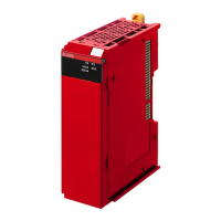
CJ1W-ID231 DC Input Unit (24 VDC, 32 Points)
Name 32-point DC Input Unit with Fujitsu Connector
Model CJ1W-ID231
Rated Input Voltage 24 VDC
Allowable Input Voltage
Range
20.4 to 26.4 VDC
Input Impedance 5.6 k
Input Current 4.1 mA typical (at 24 VDC)
ON Voltage/ON Current 19.0 VDC min./3 mA min.
OFF Voltage/OFF Current 5 VDC max./1 mA max.
ON Response Time
8.0 ms max. (Can be set to between 0 and 32 ms in the Unit Information settings.)
*
OFF Response Time
8.0 ms max. (Can be set to between 0 and 32 ms in the Unit Information settings.)
*
Number of Circuits 32 (16 points/common, 2 circuits)
Number of Simultaneously
ON Points
75% (12 points/common) simultaneously ON (at 24 VDC) (Refer to the following illustration.)
Insulation Resistance 20 M between external terminals and the GR terminal (100 VDC)
Dielectric Strength
1,000 VAC between the external terminals and the GR terminal for 1 minute at a leakage current of 10 mA
max.
Internal Current Consump-
tion
90 mA max.
Weight 70 g max.
Accessories None
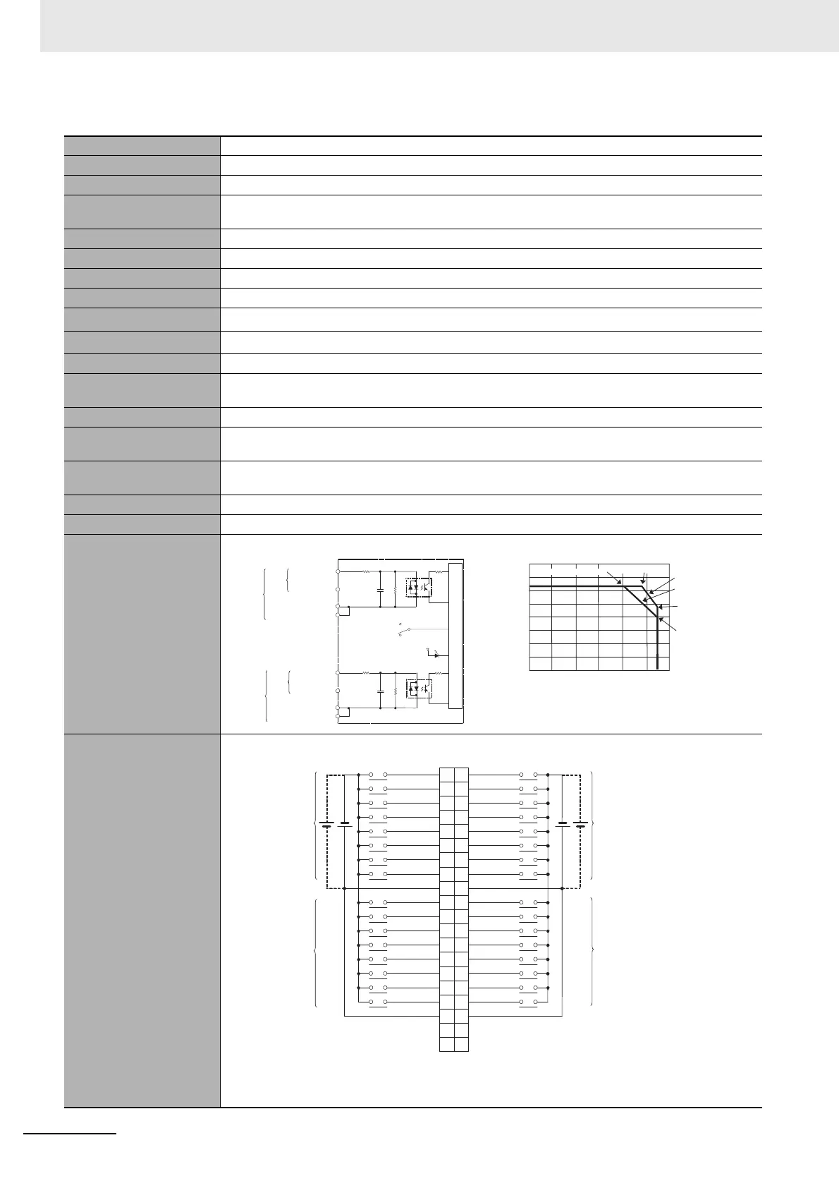
Circuit Configuration
External connection and
terminal-device variable
diagram
• The input power polarity can be connected in either direction.
• Be sure to wire both pins A9 and A18 (COM0), and set the same polarity for both pins.
• Be sure to wire both pins B9 and B18 (COM1), and set the same polarity for both pins.
560 Ω
560 Ω
5.6 kΩ
5.6 kΩ
1000 pF1000 pF
Internal circuits
Input indicator
to
to
Wd
m+1
Wd m
Allocated
CIO word
Signal
name
Connector
row A
Connector
row B
Jxx_Ch1_In00
Jxx_Ch1_In15
COM0
Jxx_Ch2_In00
Jxx_Ch2_In15
COM1
COM0
COM1
SW
0
5
10
15
20
25
30
35
010 20 30 40 5060
Number of Simultaneously ON Points vs.
Ambient Temperature Characteristic
Number of simultaneously ON points
Ambient Temperature
(°C)
10 points/
common
at 55°C
12 points/
common
at 55°C
Input voltage:
26.4 VDC
Input voltage:
24 VDC
32 points at 48°C
32 points at 40°C
Allocated
CIO word
Allocated
CIO word
Wd m+1
Wd m
24
VDC
Wd m
Wd m+1
24
VDC
Signal
name
Signal
name
Connec-
tor pin
Jxx_Ch1_In00
Jxx_Ch1_In01
Jxx_Ch1_In02
Jxx_Ch1_In03
Jxx_Ch1_In04
Jxx_Ch1_In05
Jxx_Ch1_In06
Jxx_Ch1_In07
Jxx_Ch2_In00
Jxx_Ch2_In01
Jxx_Ch2_In02
Jxx_Ch2_In03
Jxx_Ch2_In04
Jxx_Ch2_In05
Jxx_Ch2_In06
Jxx_Ch2_In07
COM0
Jxx_Ch1_In08
Jxx_Ch1_In09
Jxx_Ch1_In10
Jxx_Ch1_In11
Jxx_Ch1_In12
Jxx_Ch1_In13
Jxx_Ch1_In14
Jxx_Ch1_In15
Jxx_Ch2_In08
Jxx_Ch2_In09
Jxx_Ch2_In10
Jxx_Ch2_In11
Jxx_Ch2_In12
Jxx_Ch2_In13
Jxx_Ch2_In14
Jxx_Ch2_In15
COM0
NC
NC
COM1
COM1
NC
NC
A1
A2
A3
A4
A5
A6
A7
A8
A9
A10
A11
A12
A13
A14
A15
A16
A17
A18
A19
A20
B1
B2
B3
B4
B5
B6
B7
B8
B9
B10
B11
B12
B13
B14
B15
B16
B17
B18
B19
B20
 Loading...