6 Connection
−32−
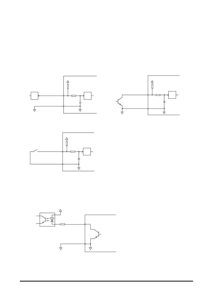
6.4 Driver I/O circuit and example connection
Input signal
The driver’s signal input is a C-MOS input. The signal status indicates “0 to 0.5 V (L
level) when ON,” or “4 to 5 V (H level) when OFF.”
• External control device output is a 5 V
C-MOS output
+5 V C-MOS
0.1 µF
2.2 kΩ
GND
+5 V
10 kΩ
START/STOP
RUN/BRAKE
CW/CCW
INT.VR/EXT
ALARM-RESET
C-MOS
Driver internal connections
0 V
0 V
• External control device output is an
open-collector output
0.1 µF
2.2 kΩ
GND
+5 V
10 kΩ
START/STOP
RUN/BRAKE
CW/CCW
INT.VR/EXT
ALARM-RESET
C-MOS
Open
collector
Driver internal connections
0 V
0 V
• Switch connection
0.1 µF
2.2 kΩ
GND
+5 V
10 kΩ
START/STOP
RUN/BRAKE
CW/CCW
INT.VR/EXT
ALARM-RESET
C-MOS
Switch
Driver internal connections
0 V
Output signal
The driver’s signal output is a transistor open-collector output. The signal status
does not indicate the voltage level of the signal, but it indicates “ON (energized)” or
“OFF (not energized)” of the internal transistor.
GND
2SC2458 or equivalent
Driver internal connections
Insert a resistor
to keep the current
to 10 mA or less
+26.4 V or less
10 mA or less
SPEED
ALARM
0 V
0 V
 Loading...