LTE Standard Module Series
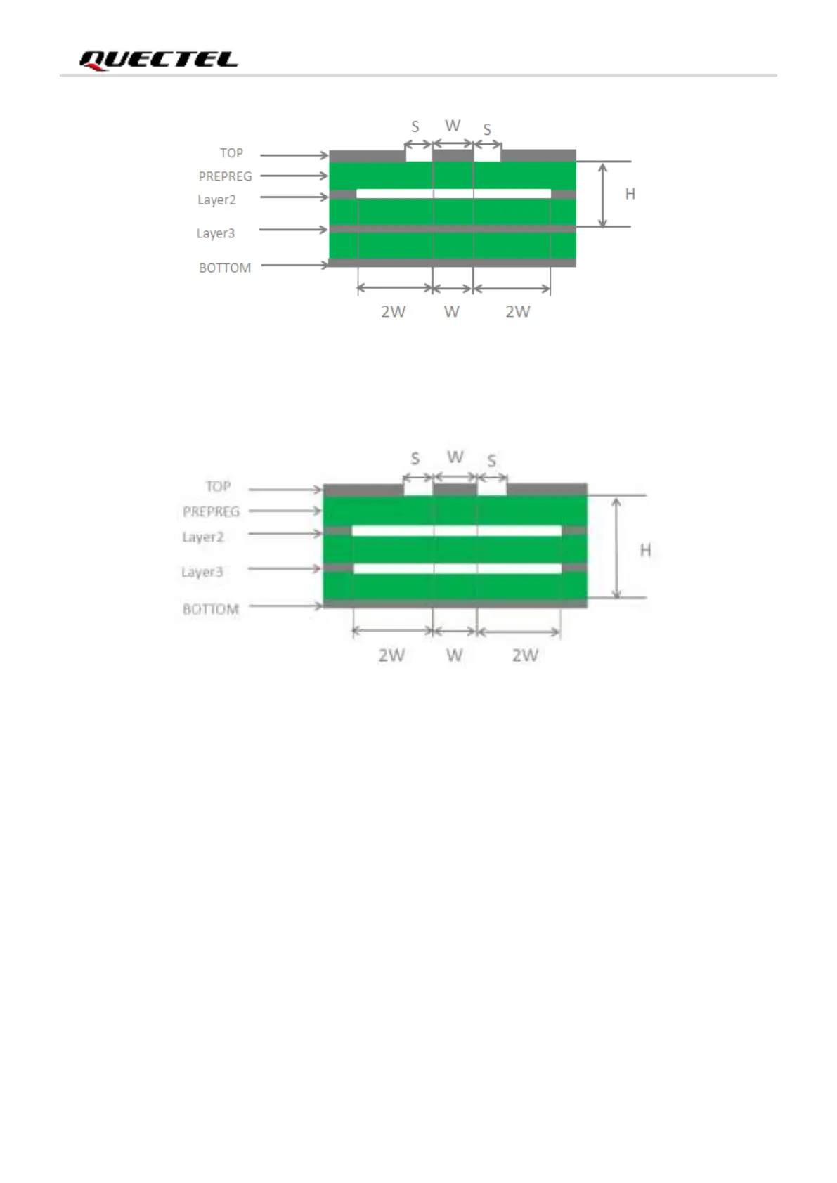
Figure 31: Coplanar Waveguide Design on a 4-layer PCB (Layer 3 as Reference Ground)
Figure 32: Coplanar Waveguide Design on a 4-layer PCB (Layer 4 as Reference Ground)
In order to ensure RF performance and reliability, the following principles should be complied with in RF
layout design:
⚫ Use an impedance simulation tool to accurately control the characteristic impedance of RF traces to
50 Ω.
⚫ The GND pins adjacent to RF pins should not be designed as thermal relief pads, and should be fully
connected to ground.
⚫ The distance between the RF pins and the RF connector should be as short as possible, and all the
right-angle traces should be changed to curved ones.
⚫ There should be clearance under the signal pin of the antenna connector or solder joint.
⚫ The reference ground of RF traces should be complete. Meanwhile, ground vias around RF traces
and the reference ground improves RF performance. The distance between the ground vias and RF
traces should be more than two times the width of RF signal traces (2 × W).
⚫ Keep RF traces away from interference sources, and avoid intersection and paralleling between

 Loading...