LTE-A Module Series
EG06 Hardware Design
EG06_Hardware_Design 45 / 89
For more details about the USB 2.0&3.0 specifications, please visit http://www.usb.org/home.
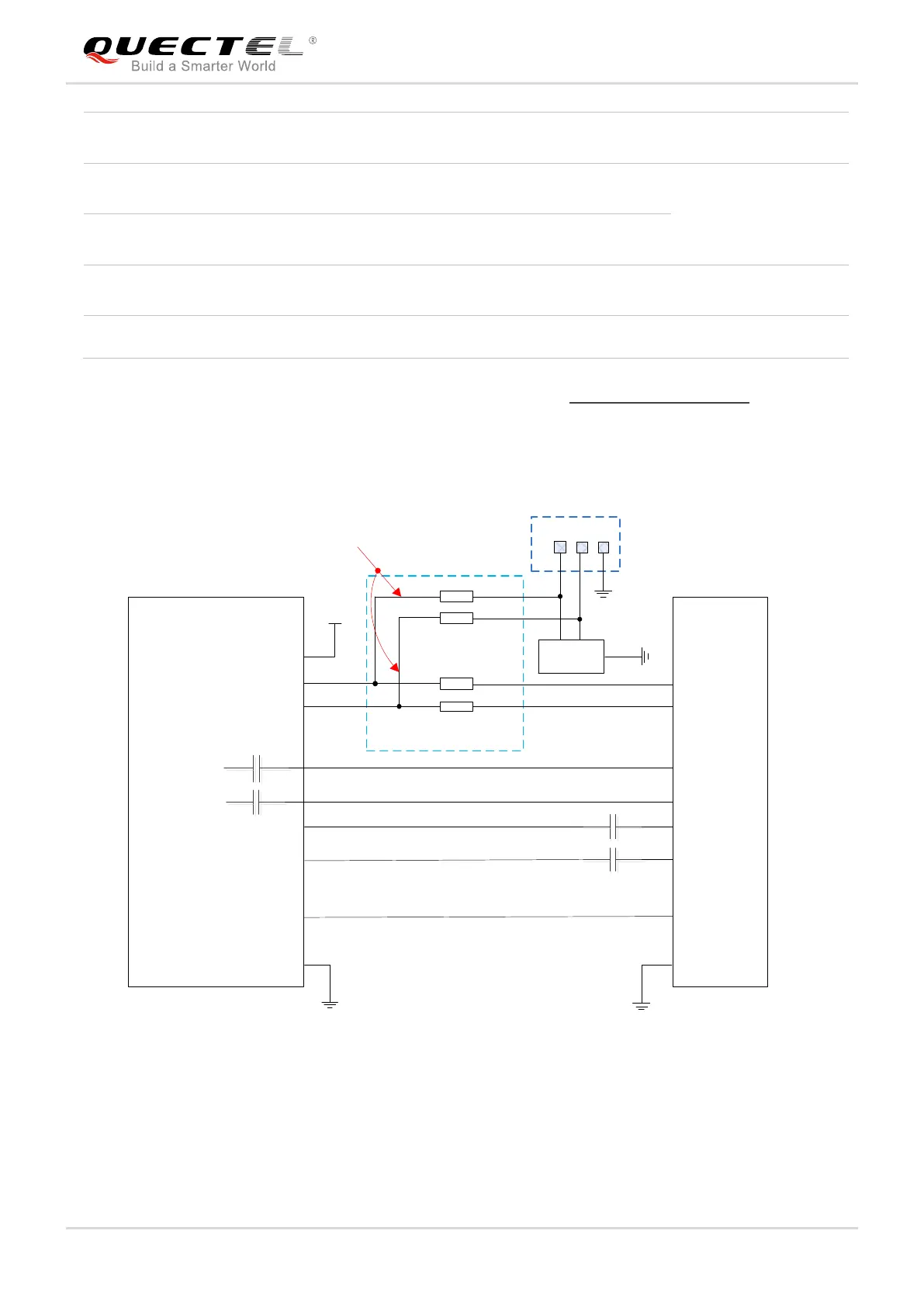
The USB interface is recommended to be reserved for firmware upgrade in customers’ designs. The
following figure shows a reference circuit of USB 2.0 & USB 3.0 interface.
USB_DP
USB_DM
GND
USB_DP
USB_DM
GND
R1
R2
Close to Module
R3
R4
Test Points
ESD Array
NM_0R
NM_0R
0R
0R
Minimize these stubs
Module
MCU
USB_VBUS
VDD
USB_SS_TX_P
USB_SS_TX_M
USB_SS_RX_P
USB_SS_RX_M
C1
C2
C3
C4
100nF
100nF
100nF
100nF
USB_SS_RX_P
USB_SS_RX_M
USB_SS_TX_P
USB_SS_TX_M
USB_ID GPIO
Figure 20: Reference Circuit of USB Application
In order to ensure the signal integrity of USB data lines, components R1, R2, R3, R4 must be placed
close to the module, the two capacitors of C1 and C2 have been placed inside the module,C3 and C4
components must be placed close to the MCU, and also these resistors should be placed close to each
USB 3.0 super-speed transmit - minus
USB 3.0 super-speed receive -plus
Require differential
impedance of 90Ω
USB 3.0 super-speed receive -minus

 Loading...