LTE-A Module Series
EG06 Hardware Design
EG06_Hardware_Design 66 / 89
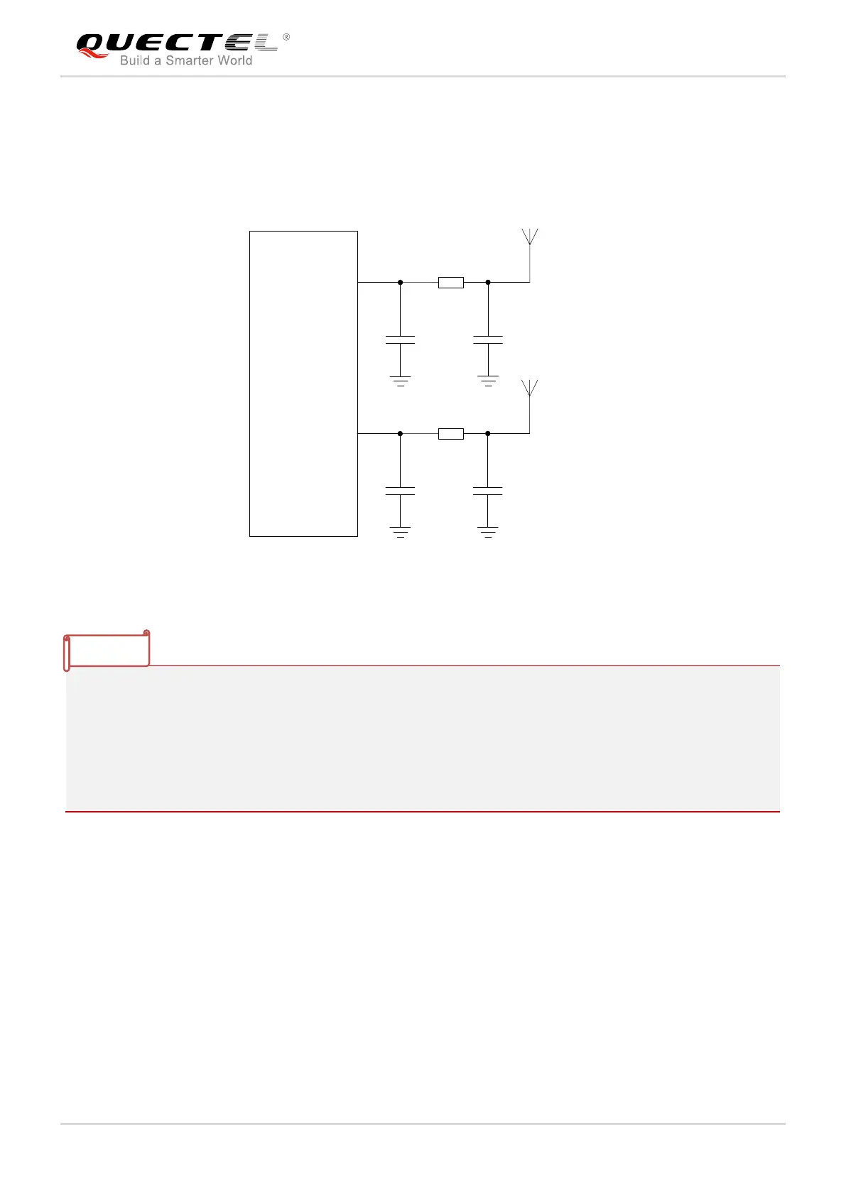
5.1.3. Reference Design of RF Antenna Interface
A reference design of ANT_MAIN and ANT_DIV antenna pads is shown as below. It should reserve a
π-type matching circuit for better RF performance. The capacitors are not mounted by default.
1. Keep a proper distance between the main antenna and the Rx-diversity antenna to improve the
receiving sensitivity.
2. ANT_DIV function is enabled by default. AT+QCFG="diversity",0 command can be used to disable
receive diversity.
3. Place the π-type matching components (R1/C1/C2 and R2/C3/C4) as close to the antenna as
possible.
5.1.4. Reference Design of RF Layout
For user’s PCB, the characteristic impedance of all RF traces should be controlled as 50Ω. The
impedance of the RF traces is usually determined by the trace width (W), the materials’ dielectric constant,
the distance between signal layer and reference ground (H), and the clearance between RF trace and
ground(S). Microstrip line or coplanar waveguide line is typically used in RF layout for characteristic
impedance control. The following are reference designs of microstrip line or coplanar waveguide line with
different PCB structures.

 Loading...