LTE-A Module Series
EG06 Hardware Design
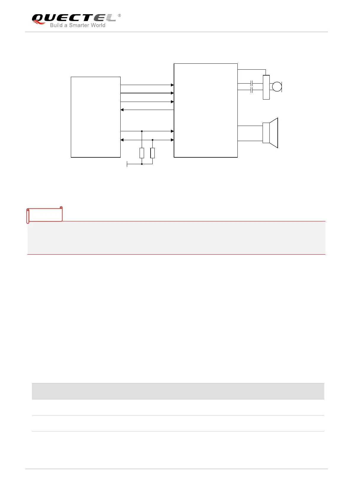
EG06_Hardware_Design 51 / 89
The following figure shows a reference design of PCM interface with an external codec IC.
PCM_IN
PCM_OUT
PCM_SYNC
PCM_CLK
I2C_SCL
I2C_SDA
Module
1.8V
4.7K
4.7K
BCLK
LRCK
DAC
ADC
SCL
SDA
BIAS
MICBIAS
INP
INN
LOUTP
LOUTN
Codec
Figure 25: Reference Circuit of PCM Application with Audio Codec
1. It is recommended to reserve an RC (R=22Ω, C=22pF) circuit on the PCM lines, especially for
PCM_CLK.
2. EG06 works as a master device pertaining to I2C interface.
3.13. ADC Interfaces
The module provides two Analog-to-Digital Converters (ADC) interfaces. AT+QADC=0 command can be
used to read the voltage value on ADC0 pin. AT+QADC=1 command can be used to read the voltage
value on ADC1 pin. For more details about these AT+QADC command, please refer to document [1].
In order to improve the accuracy of ADC, the trace of ADC should be surrounded by ground.
Table 16: Pin Definition of the ADC Interfaces
General purpose analog to digital converter
General purpose analog to digital converter

 Loading...