LTE-A Module Series
EG06 Hardware Design
EG06_Hardware_Design 60 / 89
Table 26: Parameters of SPI Interface Timing
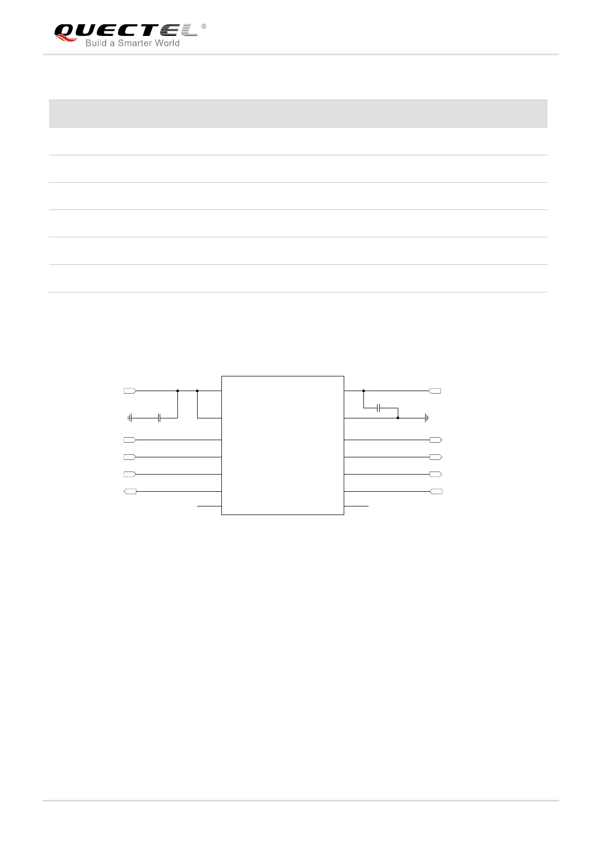
The module provides a 1.8V SPI interface. A level translator between the module and host should be
used if the application is equipped with a 3.3V processor or device interface. The following figure shows a
reference design.
VCCA VCCB
OE
A1
A2
A3
A4
NC
GND
B1
B2
B3
B4
NC
VDD_EXT
SPI_CS
SPI_CLK
SPI_MISO
SPI_MOSI
0.1uF
0.1uF
SPI_CS_N_MCU
SPI_CLK_MCU
SPI_MISO_MCU
SPI_MOSI_MCU
VDD_MCU
Translator
Figure 30: SPI Interface Reference Circuit with a Level Translator
3.21. USB_BOOT Interface
EG06 provides a USB_BOOT pin. Developers can pull up USB_BOOT to VDD_EXT before powering on
the module, thus the module will enter into emergency download mode when powered on. In this mode,
the module supports firmware upgrade over USB interface.
SPI clock high level time
SPI master data output valid time
SPI master data input setup time
SPI master data input hold time

 Loading...