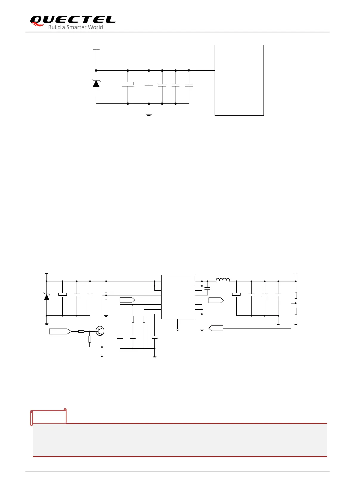
Figure 4: Reference Design of VCC
3.4.2. Reference Design of Power Supply
Power design is critical as the module’s performance largely depends on its power source. The power
supply should be capable of providing a sufficient current of 2 A at least. If the voltage drop between the
input and output is not too big, it is suggested that an LDO is used while supplying power for the module;
If there is a big voltage difference between the input source and the desired output (VCC = 3.7 V Typ.), a
buck DC-DC converter is preferred.
The following figure shows a reference design of a +5 V input power source with the DC-DC TPS54319.
The typical output of the power supply is about 3.7 V and the maximum load current is 3 A.
In order to avoid damages to the internal flash, please do not switch off the power supply directly when
the module is working. It is suggested that the power supply be cut off after pulling down the
FULL_CARD_POWER_OFF# pin for about 100 ms.
 Loading...