LTE-A Module Series
EM06 Series Hardware Design
EM06_Series_Hardware_Design 62 / 69
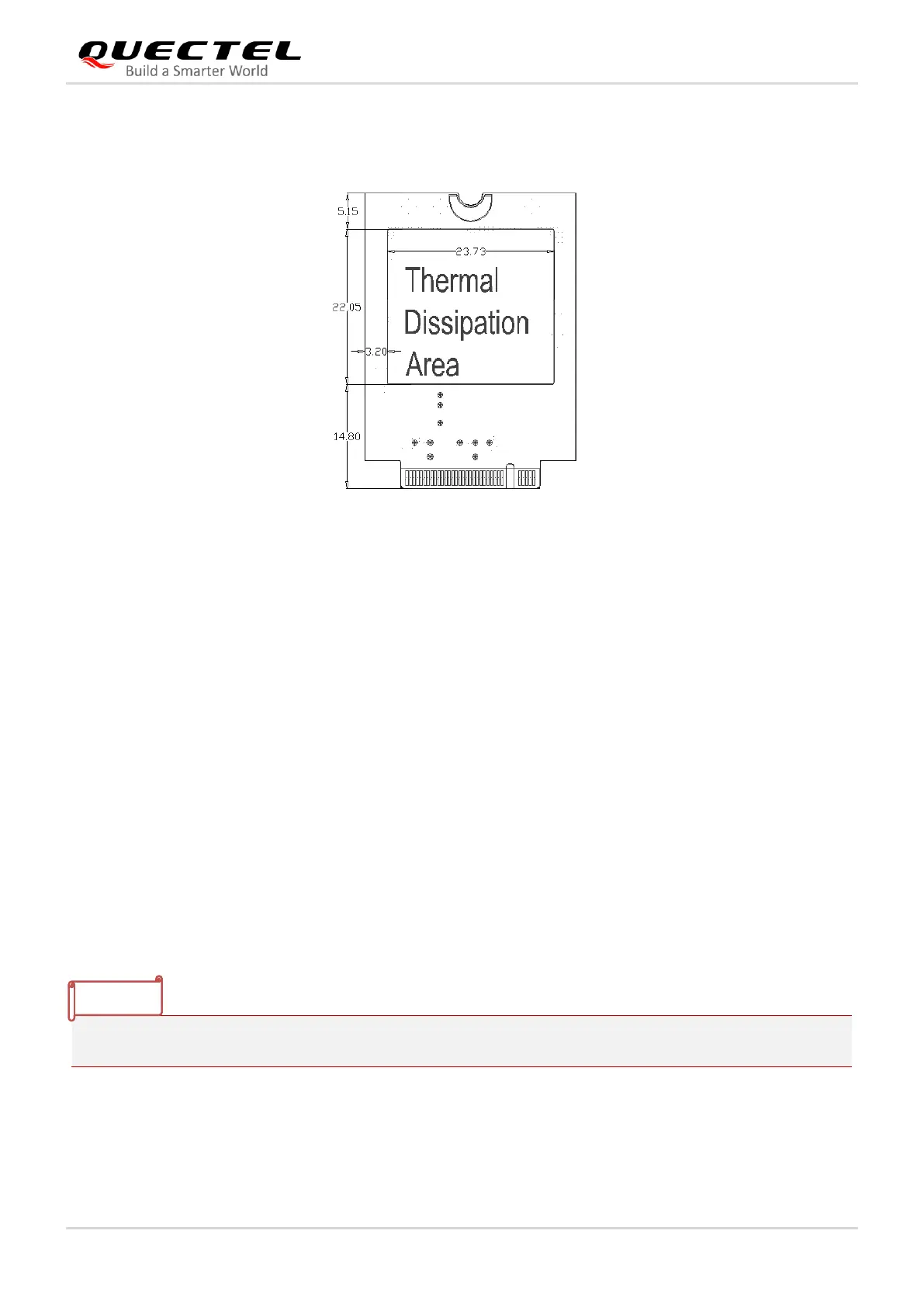
The thermal dissipation area, where the thermal pad is added, is shown as below. The dimensions are
measured in mm.
Figure 30: Thermal Dissipation Area on Bottom Side of Module (Top View)
There are some other measures to enhance heat dissipation performance:
⚫ Add as many ground vias as possible on the PCB.
⚫ Maximize the airflow over/around the module.
⚫ Place the module away from other heating sources.
⚫ Module mounting holes must be used to attach (ground) the device to the main PCB ground.
⚫ It is NOT recommended to apply solder mask on the main PCB where the module’s thermal
dissipation area is located.
⚫ To facilitate thermal dissipation, select an appropriate piece of material with suitable thickness and
surface for the outer housing (i.e. the mechanical enclosure) of the application device that integrates
the module.
⚫ Use active cooling method when necessary to pull heat away from the module.
⚫ Add a heatsink on the top of the module when possible. In that case, a thermal pad should be used
between the heatsink and the module with the former being designed to have as many fins as
possible to increase the heat dissipation area.
 Loading...