E1/E20/E2/E2 Lite Additional Document 3. Notes on Usage
R20UT2937EJ0301 Rev.3.01 Page 36 of 45
Jul 1, 2020
3.3 MCU Resources to be Occupied
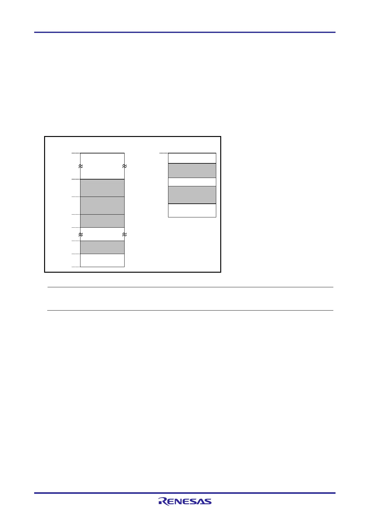
Figure 3-1 shows the areas which are occupied by the E1/E20/E2/E2 Lite for debugging.
These areas (shaded sections) are used for debugging. These areas should not be changed to save the
user program or data. If a change is made, control by the E1/E20/E2/E2 Lite is no longer possible.
However, when "No" is selected in the [Permit flash programming] property of the debugger, the internal
ROM spaces shown in Figure 3-1 are not used (only the internal RAM spaces are used).
When selecting not to permit flash memory rewriting with the debugger's property, also refer to section
3.3.3, Setting an On-Chip Debugging Option Byte.
00000h
Security ID area
10 bytes
000C3h
Reset vector area
2 bytes
00002h
Debug monitor area
2 bytes
00004h
On-chip debug
option byte area
1 byte
000C4h
000CEh
Debug monitor area
10 bytes
000D8h
Stack area for debugging
10 bytes
Area for pseudo-RRM/
pseudo-DMM
4 bytes
Internal
ROM end
address
Internal ROM
space
Internal
RAM end
address
Internal RAM
space
Figure 3-1 MCU Resources to be Occupied
*1 The reset vector area is used by the program for the E1/E20/E2/E2 Lite when performing debugging
with the E1/E20/E2/E2 Lite. If the contents of the reset vector area are changed, control by the
E1/E20/E2/E2 Lite is no longer possible.
3.3.1 Securing an Area for the Debugging Monitor Program
You may need to secure the area to which the debugging monitor program is to be allocated. The
monitor program initializes the debugger communications interface and handles processing to make the
CPU run or break execution.
The user program or data must not be placed within 23 bytes of the on-chip debugging option byte.
In addition, the reset vector must be changed if it points to an address to which the monitor program is
allocated.
The working RAM for the pseudo-RRM/pseudo-DMM starts at addresses 0x02 and 0x03.
The internal ROM spaces, including the debug monitoring area, are erased when the debugger is
closed.
[Securing the area]
Specifically securing the area for the monitor program is not necessarily required if the user program
does not use the area.
However, to avoid problems that may occur while the debugger is starting up, we recommend securing
this area in advance by using a build tool or some other means.