R8C/1A Group, R8C/1B Group 14. Timers
Rev.1.30 Dec 08, 2006 Page 149 of 315
REJ09B0252-0130
14.3.2 Output Compare Mode
In output compare mode, an interrupt request is generated when the value of the TC register matches the value
of the TM0 or TM1 register. Table 14.12 shows the Output Compare Mode Specifications. Figure 14.31 shows
an Operating Example in Output Compare Mode.
NOTES:
1. When the corresponding port data is 1, the waveform is output depending on the setting of the
registers TCC1 and TCOUT. When the corresponding port data is 0, the fixed level is output (refer to
Figure 14.25 Block Diagram of CMP Waveform Output Unit).
2. Access registers TC, TM0, and TM1 in 16-bit units.
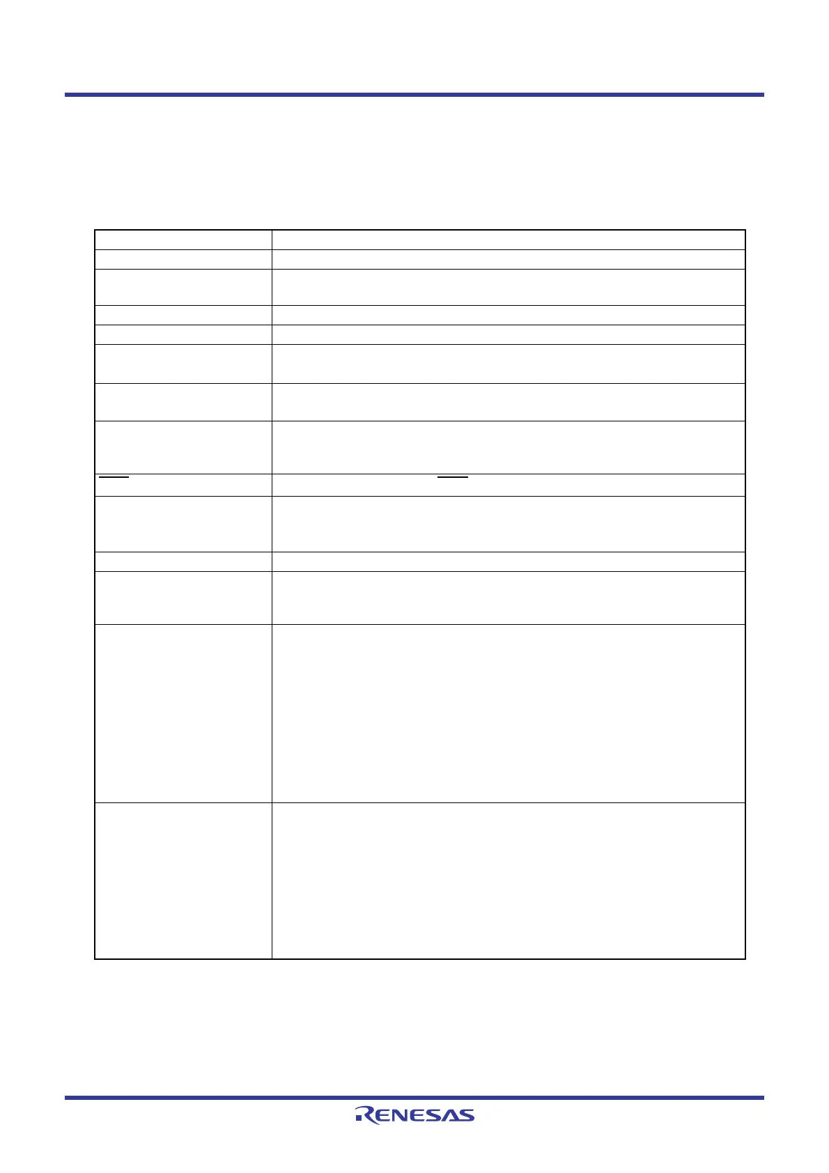
Table 14.12 Output Compare Mode Specifications
Item Specification
Count sources f1, f8, f32, fRING-fast
Count operations • Increment
• The value in the TC register is set to 0000h when the count stops.
Count start condition The TCC00 bit in the TCC0 register is set to 1 (count starts).
Count stop condition The TCC00 bit in the TCC0 register is set to 0 (count stops).
Waveform output start
condition
Bits TCOUT0 to TCOUT5 in the TCOUT register are set to 1 (enables CMP
output).
(2)
Waveform output stop
condition
Bits TCOUT0 to TCOUT5 in the TCOUT register are set to 0 (disables CMP
output).
Interrupt request
generation timing
• When a match occurs in compare circuit 0 [compare 0 interrupt].
• When a match occurs in compare circuit 1 [compare 1 interrupt].
• When time C overflows [timer C interrupt].
INT3
/TCIN pin function Programmable I/O port or INT3 interrupt input
P1_0 to P1_2 pins and
P3_3 to P3_5 pins
functions
Programmable I/O port or CMP output
(1)
Counter value reset timing When the TCC00 bit in the TCC0 register is set to 0 (count stops).
Read from timer
(2)
• The value in the compare register can be read out by reading registers
TM0 and TM1.
• The count value can be read out by reading the TC register.
Write to timer
(2)
• Write to the TC register is disabled.
• The values written to registers TM0 and TM1 are stored in the compare
register in the following timings:
- When registers TM0 and TM1 are written to, if the TCC00 bit is set to 0
(count stops).
- When the counter overflows, if the TCC00 bit is set to 1 (during counting)
and the TCC12 bit in the TCC1 register is set to 0 (free-run).
- When the compare 1 matches a counter, if the TCC00 bit is set to 1 and
the TCC12 bit is set to 1 (the TC register is set to 0000h at compare 1
match).
Select functions • Timer C counter reload select function
The TCC12 bit in the TCC1 register can select whether the counter value
in the TC register is set to 0000h when the compare circuit 1 matches.
• Bits TCC14 to TCC15 in the TCC1 register can be used to select the
output level when compare circuit 0 matches. Bits TCC16 to TCC17 in the
TCC1 register can be used to select the output level when compare circuit
1 matches.
• Bits TCOUT6 to TCOUT7 in the TCOUT register can select whether the
output is inverted or not.
 Loading...


