R8C/1A Group, R8C/1B Group 19. Electrical Characteristics
Rev.1.30 Dec 08, 2006 Page 276 of 315
REJ09B0252-0130
19. Electrical Characteristics
NOTES:
1. V
CC = 2.7 to 5.5 V at Topr = -20 to 85 °C / -40 to 85 °C, unless otherwise specified.
2. Typical values when average output current is 100 ms.
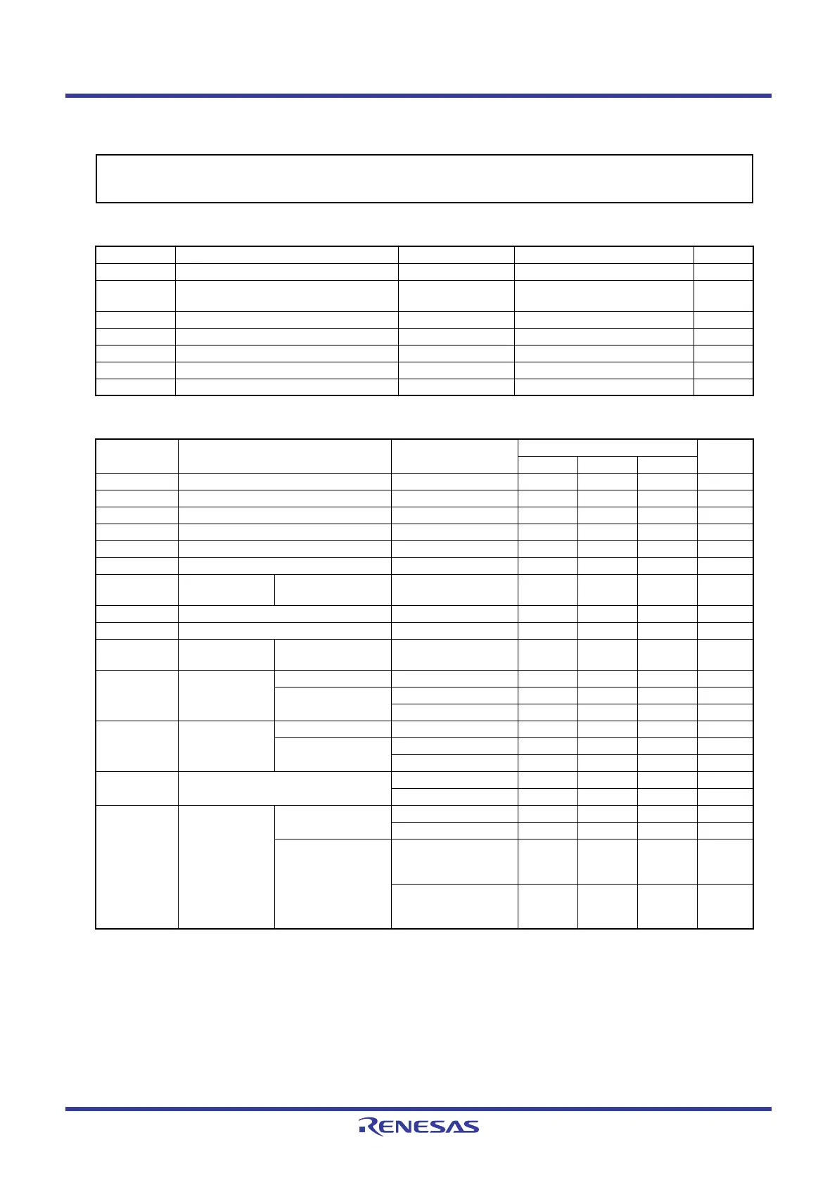
Table 19.1 Absolute Maximum Ratings
Symbol Parameter Condition Rated Value Unit
V
CC Supply voltage VCC = AVCC -0.3 to 6.5 V
AV
CC Analog supply voltage VCC = AVCC -0.3 to 6.5 V
V
I Input voltage -0.3 to VCC+0.3 V
V
O Output voltage -0.3 to VCC+0.3 V
P
d Power dissipation Topr = 25°C300mW
T
opr Operating ambient temperature -20 to 85 / -40 to 85 (D version) °C
T
stg Storage temperature -65 to 150 °C
Table 19.2 Recommended Operating Conditions
Symbol Parameter Conditions
Standard
Unit
Min. Typ. Max.
V
CC Supply voltage 2.7 − 5.5 V
AV
CC Analog supply voltage − VCC − V
V
SS Supply voltage − 0 − V
AV
SS Analog supply voltage − 0 − V
V
IH Input “H” voltage 0.8VCC − VCC V
V
IL Input “L” voltage 0 − 0.2VCC V
I
OH(sum) Peak sum output
“H” current
Sum of all pins
I
OH(peak)
−−-60 mA
I
OH(peak) Peak output “H” current −−-10 mA
I
OH(avg) Average output “H” current −−-5 mA
I
OL(sum) Peak sum output
“L” currents
Sum of all pins
I
OL(peak)
−−60 mA
I
OL(peak) Peak output “L”
currents
Except P1_0 to P1_3 −−10 mA
P1_0 to P1_3 Drive capacity HIGH
−−30 mA
Drive capacity LOW
−−10 mA
I
OL(avg) Average output
“L” current
Except P1_0 to P1_3 −−5mA
P1_0 to P1_3 Drive capacity HIGH
−−15 mA
Drive capacity LOW
−−5mA
f
(XIN) Main clock input oscillation frequency 3.0 V ≤ VCC ≤ 5.5 V 0 − 20 MHz
2.7 V
≤ VCC < 3.0 V 0 − 10 MHz
− System clock OCD2 = 0
Main clock selected
3.0 V ≤ VCC ≤ 5.5 V 0 − 20 MHz
2.7 V
≤ VCC < 3.0 V 0 − 10 MHz
OCD2 = 1
On-chip oscillator
clock selected
HRA01 = 0
Low-speed on-chip
oscillator clock selected
− 125 − kHz
HRA01 = 1
High-speed on-chip
oscillator clock selected
− 8 − MHz
Please contact Renesas Technology sales offices for the electrical characteristics in the Y version (Topr =
-20°C to 105°C ).
 Loading...


