R8C/1A Group, R8C/1B Group 19. Electrical Characteristics
Rev.1.30 Dec 08, 2006 Page 277 of 315
REJ09B0252-0130
NOTES:
1. V
CC = AVCC = 2.7 to 5.5 V at Topr = -20 to 85 °C / -40 to 85 °C, unless otherwise specified.
2. If f1 exceeds 10 MHz, divide f1 and ensure the A/D operating clock frequency (
φAD) is 10 MHz or below.
3. If AVcc is less than 4.2 V, divide f1 and ensure the A/D operating clock frequency (
φAD) is f1/2 or below.
4. When the analog input voltage is over the reference voltage, the A/D conversion result will be 3FFh in 10-bit mode and FFh in
8-bit mode.
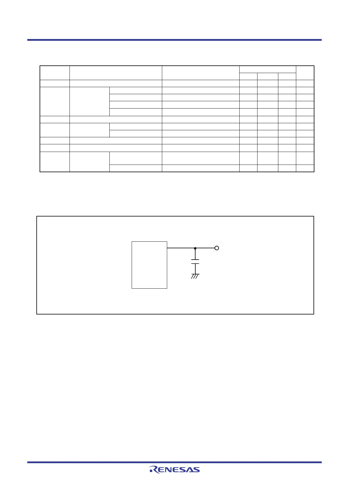
Figure 19.1 Port P1, P3, and P4 Measurement Circuit
Table 19.3 A/D Converter Characteristics
Symbol Parameter Conditions
Standard
Unit
Min. Typ. Max.
− Resolution Vref = VCC −−10 Bits
− Absolute
accuracy
10-bit mode φAD = 10 MHz, Vref = VCC = 5.0 V −−±3 LSB
8-bit mode
φAD = 10 MHz, Vref = VCC = 5.0 V −−±2 LSB
10-bit mode
φAD = 10 MHz, Vref = VCC = 3.3 V
(3)
−−±5 LSB
8-bit mode
φAD = 10 MHz, Vref = VCC = 3.3 V
(3)
−−±2 LSB
R
ladder Resistor ladder Vref = VCC 10 − 40 kΩ
tconv Conversion time 10-bit mode φAD = 10 MHz, Vref = VCC = 5.0 V 3.3 −−µs
8-bit mode
φAD = 10 MHz, Vref = VCC = 5.0 V 2.8 −−µs
V
ref Reference voltage 2.7 − Vcc V
V
IA
Analog input voltage
(4)
0 − AVcc V
− A/D operating
clock
frequency
(2)
Without sample and
hold
0.25 − 10 MHz
With sample and hold 1
− 10 MHz
P1
P3
P4
30pF
 Loading...


