R8C/1A Group, R8C/1B Group 16. Clock Synchronous Serial Interface
Rev.1.30 Dec 08, 2006 Page 226 of 315
REJ09B0252-0130
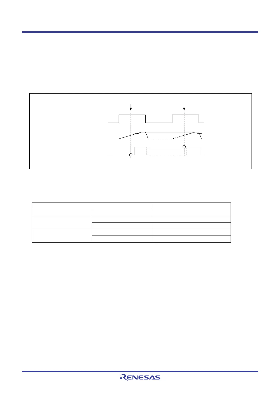
16.3.6 Bit Synchronization Circuit
When setting the I
2
C bus interface to master mode, the high-level period may become shorter in the following
two cases:
• If the SCL signal is driven L level by a slave device
• If the rise speed of the SCL signal is reduced by a load (load capacity or pull-up resistor) on the SCL line.
Therefore, the SCL signal is monitored and communication is synchronized bit by bit.
Figure 16.45 shows the Timing of Bit Synchronization Circuit and Table 16.8 lists the Time between Changing
SCL Signal from “L” Output to High-Impedance and Monitoring of SCL Signal.
Figure 16.45 Timing of Bit Synchronization Circuit
1Tcyc = 1/f1(s)
Table 16.8 Time between Changing SCL Signal from “L” Output to High-Impedance and
Monitoring of SCL Signal
ICCR1 Register Time for Monitoring SCL
CKS3 CKS2
0 0 7.5Tcyc
1 19.5Tcyc
1017.5Tcyc
1 41.5Tcyc
VIH
Basis clock of SCL
monitor timing
SCL
Internal SCL
 Loading...


